Pin description – Rainbow Electronics MAX1692 User Manual
Page 6
MAX1692
Low-Noise, 5.5V-Input,
PWM Step-Down Regulator
6
_______________________________________________________________________________________
NAME
FUNCTION
1
IN
Supply Voltage Input. Input range from +2.7V to +5.5V. Bypass with a 10µF capacitor.
2
BP
Supply Bypass Pin. Internally connected to IN. Bypass with a 0.1µF capacitor.
Do not
connect to an
external power source other than IN.
PIN
3
GND
Ground
4
REF
1.25V, 1.2% Reference Output. Capable of delivering 50µA to external loads. Bypass with a 0.22µF capaci-
tor to GND.
8
SHDN
Active-Low, Shutdown-Control Input. Reduces quiescent current to 0.1µA. In shutdown, output becomes
high impedance.
7
SYNC/
PWM
Oscillator Sync and Low-Noise, Mode-Control Input.
SYNC/PWM = IN (Forced PWM Mode)
SYNC/PWM = GND (PWM/PFM Mode)
An external clock signal connected to this pin allows for LX switching synchronization.
6
LIM
Current-Limit Select Input. Connect LIM to GND for 0.6A current limit or LIM to IN for 1.2A current limit.
5
FB
Feedback Input
10
PGND
Power Ground
9
LX
Inductor Connection to the Drains of the Internal Power MOSFETs
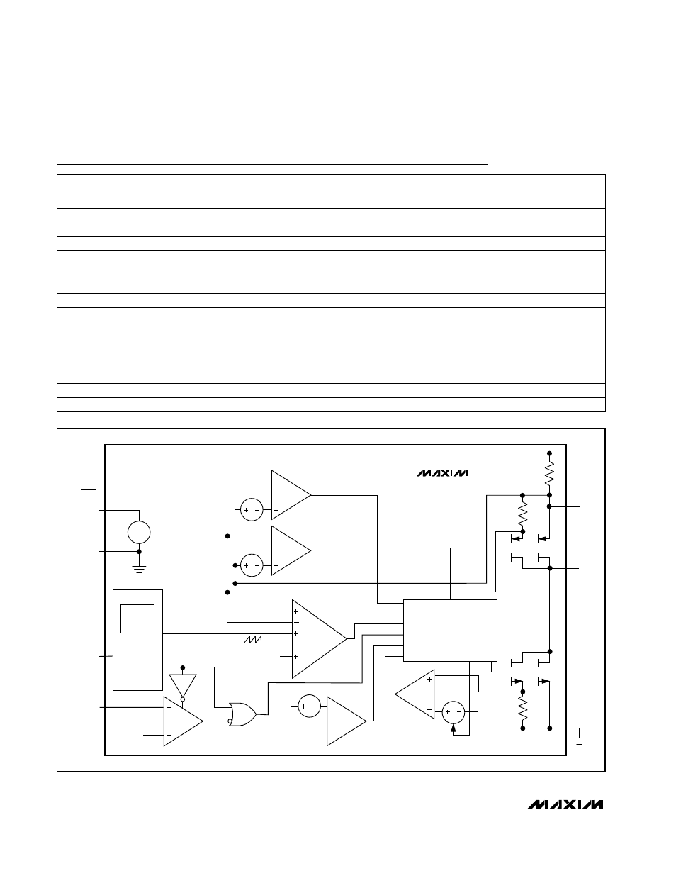
Pin Description
PFM CURRENT COMPARATOR
CONTROL AND
DRIVER LOGIC
SLOPE COMPENSATION
PWM
COMPARATOR
NEGLIM
COMPARATOR
5mV IN PFM
ADJ. IN PWM
PGND
0.1X
SENSE FET
SENSE FET
1
Ω
LX
IN
P
N
BP
0.1X
1
Ω
10
Ω
CHIP
SUPPLY
PWM
ON
REF
FB
SYNC/
PWM
PFM
COMPARATOR
OVERVOLTAGE
COMPARATOR
PWM ON
SIGNAL
40mV
FB
REF
REF
FB
12mV
120mV
RAMP
GEN
SYNC
CELL
ON
LIM COMPARATOR
REF
GND
REF
SHDN
MAX1692
Figure 1. Simplified Functional Diagram