Rainbow Electronics MAX1692 User Manual
Page 2
MAX1692
Low-Noise, 5.5V-Input,
PWM Step-Down Regulator
2
_______________________________________________________________________________________
ABSOLUTE MAXIMUM RATINGS
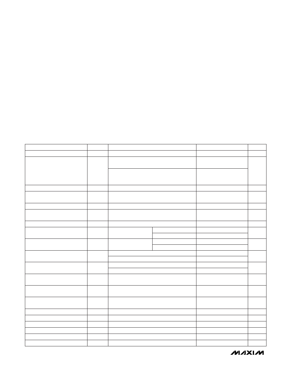
ELECTRICAL CHARACTERISTICS
(V
IN
= +3.6V, SYNC/PWM = GND, V
LIM
= 3.6V,
SHDN = IN, circuit of Figure 2;
T
A
= 0°C to +85°C
, unless otherwise noted. Typical
values are at T
A
= +25°C.)
Stresses beyond those listed under “Absolute Maximum Ratings” may cause permanent damage to the device. These are stress ratings only, and functional
operation of the device at these or any other conditions beyond those indicated in the operational sections of the specifications is not implied. Exposure to
absolute maximum rating conditions for extended periods may affect device reliability.
IN, BP, SHDN, SYNC/PWM, LIM to GND ................ -0.3V to +6V
BP to IN .................................................................-0.3V to +0.3V
PGND to GND ...................................................... -0.3V to +0.3V
LX to PGND................................................. -0.3V to (V
IN
+ 0.3V)
FB, REF to GND ......................................... -0.3V to (V
BP
+ 0.3V)
Reference Current ............................................................. ±1mA
LX Peak Current (internally limited)...................................... 1.6A
Continuous Power Dissipation (T
A
= +70°C)
10-Pin µMAX (derate 5.6mW/°C above +70°C) ............444mW
Operating Temperature Range .......................... -40°C to +85°C
Maximum Junction Temperature .................................... +150°C
Storage Temperature Range ............................ -65°C to +160°C
Lead Temperature (soldering, 10sec) .............................+300°C
(Note 1)
FB = OUT, V
IN
= V
LIM
= 2.7V to 5.5V,
I
OUT
= 0
SHDN = LX = GND, includes LX leakage
current
SYNC/PWM = GND, V
FB
= 1.4V,
LX unconnected
I
LX
= 180mA
SYNC/PWM = IN, FB = REF
V
FB
= 1.4V
V
IN
= 3.6V
FB = OUT, V
IN
= V
LIM
= 5.5V, I
OUT
= 0
(duty cycle = 23%) (Note 2)
Duty cycle = 100% to 23%
I
OUT
= 0 to 600mA, LIM = IN or
I
OUT
= 0 to 250mA, LIM = GND
LIM = IN
V
FB
= 1.4V
LIM = GND
CONDITIONS
µA
0.1
10
Shutdown Supply Current
µA
85
140
Quiescent Current
mA
80
120
160
Pulse-Skipping Current-Limit
Threshold
0
50
100
mA
-450
-850
-1600
N-Channel Current-Limit
Threshold
0.75
1.2
1.55
A
0.35
0.6
0.85
P-Channel Current-Limit
Threshold
V
V
REF
V
IN
Output Adjustment Range
1.223
1.249
1.275
V
2.7
5.5
V
IN
Input Voltage Range
0.5
Ω
0.4
0.8
N
RDS(ON)
N-Channel On-Resistance
0.4
Ω
0.3
0.65
P
RDS(ON)
P-Channel On-Resistance
V
1.223
1.249
1.275
V
FB
Feedback Voltage
%
+1
Line Regulation
%
-1.3
Load Regulation
nA
-50
0.01
50
I
FB
FB Input Current
UNITS
MIN
TYP
MAX
SYMBOL
PARAMETER
V
IN
= 5.5V, V
LX
= 0 or 5.5V
µA
-20
0.1
20
LX Leakage Current
kHz
650
750
830
f
OSC
Oscillator Frequency
kHz
500
1000
SYNC Capture Range
%
100
duty
MAX
Maximum Duty Cycle
%
22
duty
MIN
Minimum Duty Cycle
I
REF
= 0
V
1.235
1.250
1.265
V
REF
Reference Output Voltage
FB = OUT, V
IN
= 2.7V to 5.5V,
I
OUT
= 0 to 600mA, LIM = IN or
I
OUT
= 0 to 250mA, LIM = GND
V
1.190
1.232
1.275
V
OUT
Output Voltage
I
LX
= 180mA
V
IN
= 2.7V
V
IN
= 3.6V
V
IN
= 2.7V