Rainbow Electronics MAX1619 User Manual
Page 15
The address pin states are checked at POR and SPOR
only, and the address data stays latched to reduce qui-
escent supply current due to the bias current needed
for high-Z state detection. A new device address can be
written using the Write Address Command FDh.
The MAX1619 also responds to the SMBus Alert Response
slave address (see the
Alert Response Address
section).
POR and UVLO
The MAX1619 has a volatile memory. To prevent ambig-
uous power-supply conditions from corrupting the data in
memory and causing erratic behavior, a POR voltage
detector monitors V
CC
and clears the memory if V
CC
falls
below 1.7V (typical, see
Electrical Characteristics
table).
When power is first applied and V
CC
rises above 1.75V
(typical), the logic blocks begin operating, although reads
and writes at V
CC
levels below 3V are not recommended.
A second V
CC
comparator, the ADC UVLO comparator,
prevents the ADC from converting until there is sufficient
headroom (V
CC
= 2.8V typical).
The SPOR software POR command can force a power-on
reset of the MAX1619 registers via the serial interface. Use
the SEND BYTE protocol with COMMAND = FCh. This is
most commonly used to reconfigure the slave address of
the MAX1619 “on the fly,” where external hardware has
forced new states at the ADD0 and ADD1 address pins
prior to the software POR. The new address takes effect
less than 100µs after the SPOR transmission stop condition.
Power-Up Defaults:
•
Interrupt latch is cleared.
•
Address select pins are sampled.
•
ADC begins auto-converting at a 0.25Hz rate.
•
Command byte is set to 01h to facilitate quick
remote Receive Byte queries.
•
T
HIGH
and T
LOW
registers are set to +127°C and
-55°C, respectively.
•
T
MAX
and T
HYST
are set to +100°C and +95°C,
respectively.
•
OVERT polarity is active low.
MAX1619
Remote/Local Temperature Sensor with Dual-
Alarm Outputs and SMBus Serial Interface
______________________________________________________________________________________
15
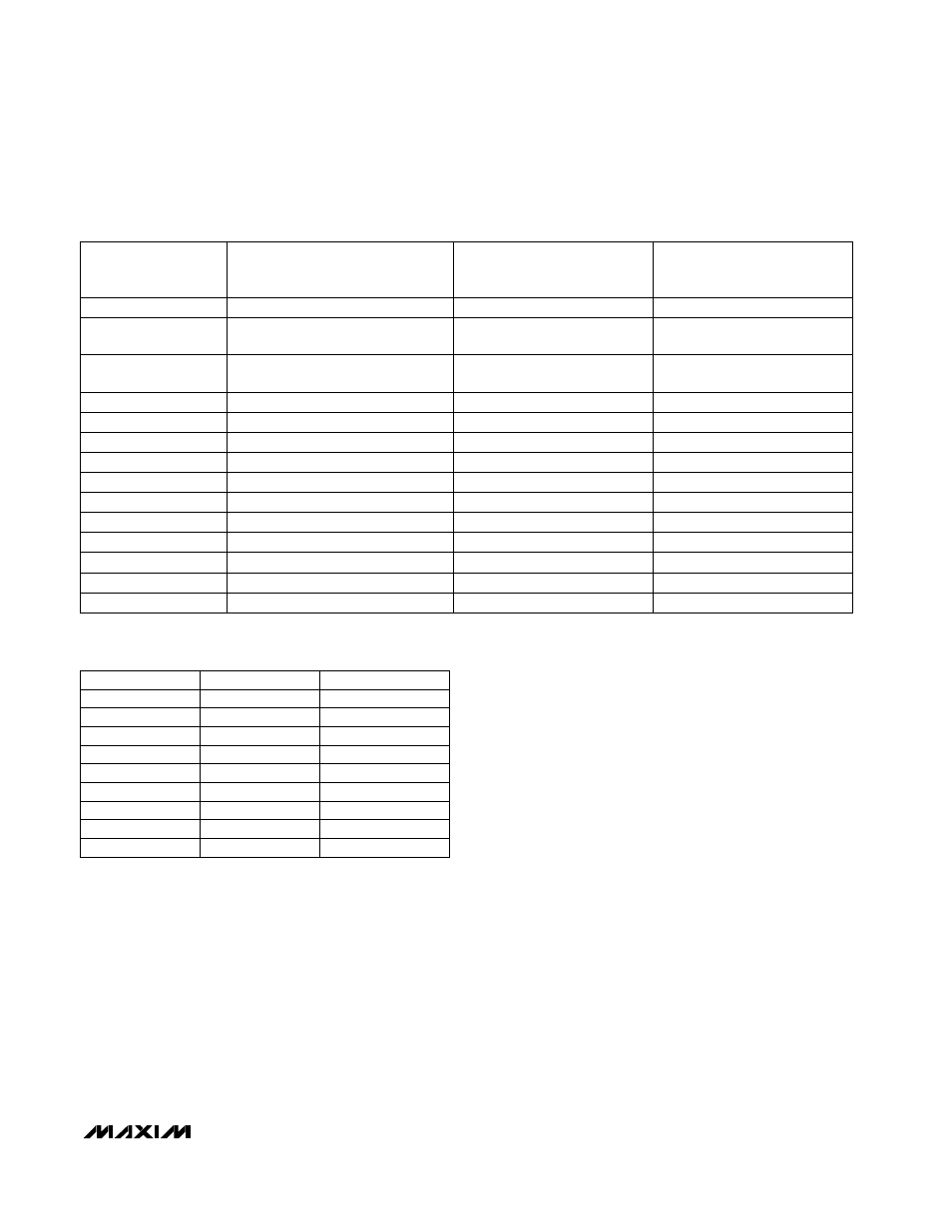
Table 8. RLTS and RRTE Temperature Register Update Timing Chart
n/a (0.25Hz)
NEW CONVERSION
FREQUENCY (CHANGED VIA
WRITE TO WCRW)
Power-on reset
Autoconvert
OPERATING MODE
CONVERSION INITIATED BY:
156ms max
TIME UNTIL RLTS AND RRTE
ARE UPDATED
156ms max
n/a
One-shot command, while idling
between automatic conversions
Autoconvert
When current conversion is
complete (1-shot is ignored)
20sec
n/a
0.0625Hz
Rate timer
Autoconvert
One-shot command that occurs
during a conversion
Autoconvert
10sec
5sec
0.125Hz
0.25Hz
Rate timer
Autoconvert
2.5sec
1.25sec
0.5Hz
1Hz
Rate timer
Autoconvert
Rate timer
Autoconvert
Rate timer
Autoconvert
625ms
312.5ms
2Hz
4Hz
Rate timer
Autoconvert
237.5ms
156ms
8Hz
n/a
STBY pin
Hardware Standby
Rate timer
Autoconvert
Rate timer
Autoconvert
156ms
156ms
n/a
n/a
One-shot command
Software Standby
RUN/STOP bit
Software Standby
Table 9. POR Slave Address Decoding
(ADD0 and ADD1)
Note:
High-Z means that the pin is left unconnected and floating.
0011 001
High-Z
GND
0011 000
ADDRESS
0101 001
GND
High-Z
0011 010
V
CC
GND
0101 011
V
CC
High-Z
0101 010
1001 101
High-Z
V
CC
1001 100
GND
GND
GND
V
CC
High-Z
High-Z
1001 110
V
CC
V
CC
ADD0
ADD1