Applications information – Rainbow Electronics MAX1209 User Manual
Page 19
Power-Down Input (PD)
The MAX1209 has two power modes that are controlled
with the power-down digital input (PD). With PD low, the
MAX1209 is in normal operating mode. With PD high,
the MAX1209 is in power-down mode.
The power-down mode allows the MAX1209 to efficient-
ly use power by transitioning to a low-power state when
conversions are not required. Additionally, the
MAX1209 parallel output bus is high impedance in
power-down mode, allowing other devices on the bus
to be accessed.
In power-down mode, all internal circuits are off, the
analog supply current reduces to 1µA, and the digital
supply current reduces to 0.9µA. The following list
shows the state of the analog inputs and digital outputs
in power-down mode:
• INP, INN analog inputs are disconnected from the
internal input amplifier (
Figure
3).
• REFOUT has approximately 17k
Ω to GND.
• REFP, COM, and REFN go high impedance with
respect to V
DD
and GND, but there is an internal 4k
Ω
resistor between REFP and COM, as well as an inter-
nal 4k
Ω resistor between REFN and COM.
• D11–D0, DOR, and DAV go high impedance.
• CLKP and CLKN go high impedance (
Figure
5).
The wake-up time from power-down mode is dominat-
ed by the time required to charge the capacitors at
REFP, REFN, and COM. In internal reference mode and
buffered external reference mode, the wake-up time is
typically 10ms with the recommended capacitor array
(
Figure
13). When operating in unbuffered external ref-
erence mode, the wake-up time is dependent on the
external reference drivers.
Applications Information
Using Transformer Coupling
In general, the MAX1209 provides better SFDR and THD
performance with fully differential input signals as
opposed to single-ended input drive. In differential input
mode, even-order harmonics are lower as both inputs are
balanced, and each of the ADC inputs only requires half
the signal swing compared to single-ended input mode.
An RF transformer (
Figure
10) provides an excellent
solution to convert a single-ended input source signal
to a fully differential signal, required by the MAX1209
for optimum performance. Connecting the center tap of
the transformer to COM provides a V
DD
/ 2 DC level
shift to the input. Although a 1:1 transformer is shown, a
step-up transformer can be selected to reduce the
drive requirements. A reduced signal swing from the
input driver, such as an op amp, can also improve the
overall distortion. The configuration of
Figure
10 is good
for frequencies up to Nyquist (f
CLK
/ 2).
MAX1209
12-Bit, 80Msps, 3.3V IF-Sampling ADC
______________________________________________________________________________________
19
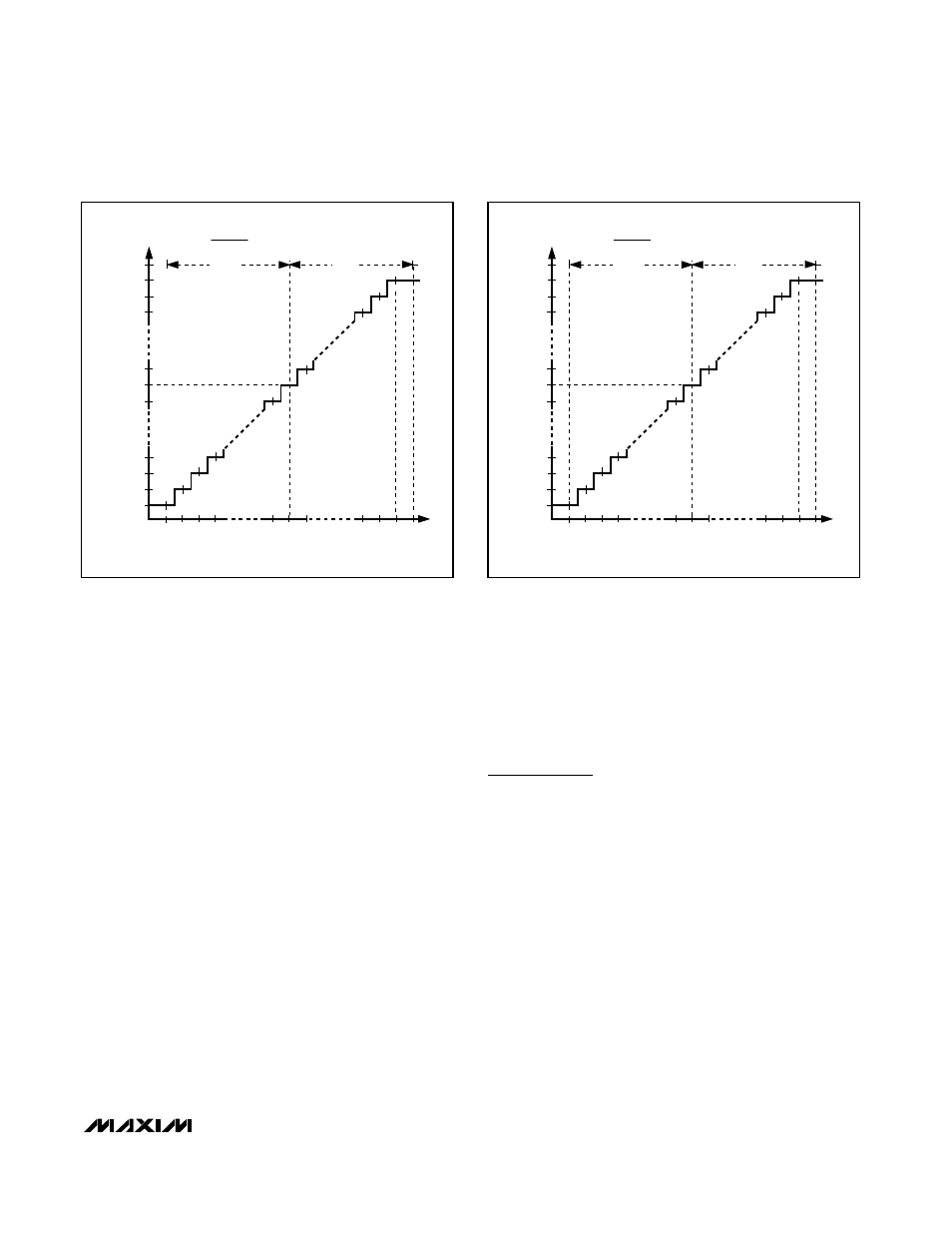
DIFFERENTIAL INPUT VOLTAGE (LSB)
-1
-2045
4096
2 x V
REF
1 LSB =
V
REF
= V
REFP
- V
REFN
V
REF
V
REF
0
+1
-2047
+2047
+2045
TWO'S COMPLEMENT OUTPUT CODE (LSB)
0x800
0x801
0x802
0x803
0x7FF
0x7FE
0x7FD
0xFFF
0x000
0x001
Figure 7. Two’s Complement Transfer Function (G/T = 0)
DIFFERENTIAL INPUT VOLTAGE (LSB)
-1
-2045
4096
2 x V
REF
1 LSB =
V
REF
= V
REFP
- V
REFN
V
REF
V
REF
0
+1
-2047
+2047
+2045
GRA
Y OUTPUT CODE (LSB)
0x000
0x001
0x003
0x002
0x800
0x801
0x803
0x400
0xC00
0xC01
Figure 8. Gray Code Transfer Function (G/T = 1)