Pin description (continued) – Rainbow Electronics MAX1209 User Manual
Page 13
MAX1209
12-Bit, 80Msps, 3.3V IF-Sampling ADC
______________________________________________________________________________________
13
PIN
NAME
FUNCTION
28
D2
CMOS Digital Output, Bit 2
29
D1
CMOS Digital Output, Bit 1
30
D0
CMOS Digital Output, Bit 0 (LSB)
31, 32
I.C.
Internally Connected. Leave I.C. unconnected.
33
DAV
Data-Valid Output. DAV is a single-ended version of the input clock that is compensated to correct for
any input clock duty-cycle variations. DAV is typically used to latch the MAX1209 output data into an
external back-end digital circuit.
37
PD
Power-Down Input. Force PD high for power-down mode. Force PD low for normal operation.
38
REFOUT
Internal Reference Voltage Output. For internal reference operation, connect REFOUT directly to REFIN
or use a resistive divider from REFOUT to set the voltage at REFIN. Bypass REFOUT to GND with a
≥0.1µF capacitor.
39
REFIN
Reference Input. In internal reference mode and buffered external reference mode, bypass REFIN to
GND with a
≥0.1µF capacitor. In these modes,V
REFP
- V
REFN
= V
REFIN
/2. For unbuffered external
reference-mode operation, connect REFIN to GND.
40
G/T
Output Format Select Input. Connect G/T to GND for the two’s complement digital output format.
Connect G/T to OV
DD
or V
DD
for the Gray code digital output format.
—
EP
Exposed Paddle. The MAX1209 relies on the exposed paddle connection for a low-inductance ground
connection. Connect EP to GND to achieve specified performance. Use multiple vias to connect the
top-side PC board ground plane to the bottom-side PC board ground plane.
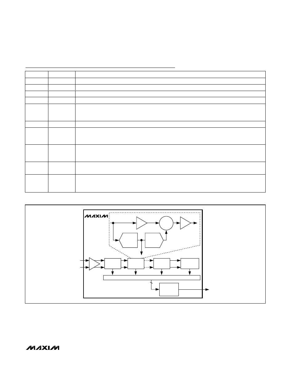
Pin Description (continued)
MAX1209
Σ
+
−
DIGITAL ERROR CORRECTION
FLASH
ADC
T/H
DAC
STAGE 2
D11–D0
INP
INN
STAGE 1
T/H
STAGE 9
STAGE 10
END OF PIPE
OUTPUT
DRIVERS
D11–D0
Figure 1. Pipeline Architecture—Stage Blocks