Rainbow Electronics MAX1848 User Manual
Page 2
MAX1848
White LED Step-Up Converter in SOT23
2
_______________________________________________________________________________________
ABSOLUTE MAXIMUM RATINGS
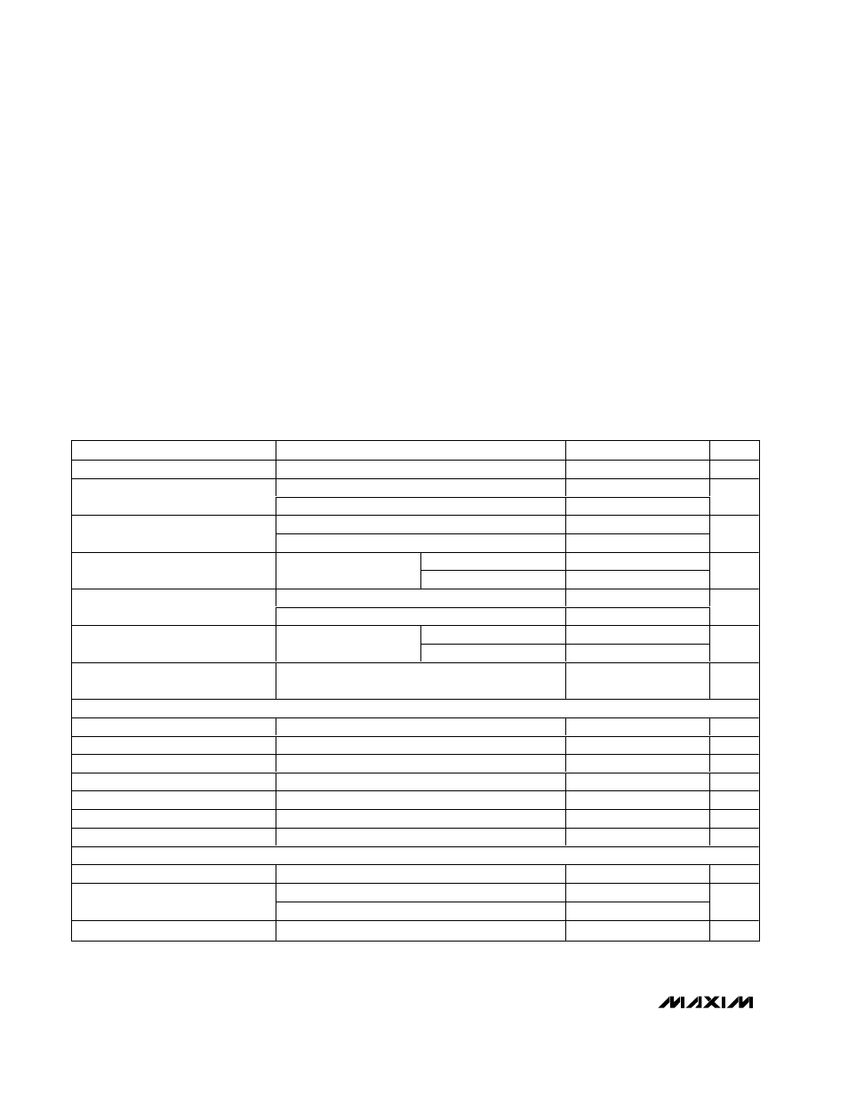
DC ELECTRICAL CHARACTERISTICS
(V+ = 3V, V
OUT
= 11V, L = 33µH, C
OUT
= 1µF, C
COMP
= 0.15µF, R
SENSE
= 5
Ω, V
CTRL
= 1V, T
A
= 0
°C to +85°C, unless otherwise
noted. Typical values are at T
A
= +25
°C.)
Stresses beyond those listed under “Absolute Maximum Ratings” may cause permanent damage to the device. These are stress ratings only, and functional
operation of the device at these or any other conditions beyond those indicated in the operational sections of the specifications is not implied. Exposure to
absolute maximum rating conditions for extended periods may affect device reliability.
V+ to GND ................................................................-0.3V to +6V
PGND to GND .......................................................-0.3V to +0.3V
LX, OUT to GND .....................................................-0.3V to +14V
LX to OUT ...............................................................-14V to +0.3V
CTRL to GND.......................................-0.3V to +6V or (V+ + 2V)
COMP, CS to GND .......................................-0.3V to (V+ + 0.3V)
LX Current ....................................................................0.45A
RMS
Continuous Power Dissipation (T
A
= +70°C)
8-Pin SOT23 (derate 9.7mW/°C above +70
°C).............777mW
8-Pin Thin QFN 3mm
✕
3mm (derate 24.4mW/°C
above +70
°C)..............................................................1951mW
Operating Temperature Range ...........................-40
°C to +85°C
Junction Temperature ......................................................+150
°C
Storage Temperature Range .............................-60
°C to +150°C
Lead Temperature (soldering, 10s) .................................+300°C
PARAMETER
CONDITIONS
MIN
TYP
MAX
UNITS
Supply Voltage
2.6
5.5
V
V+ rising, 40mV hysteresis typical
2.15
2.38
2.59
Undervoltage Lockout Threshold
V+ falling
2.10
2.34
2.56
V
Not switching, V
CTRL
= V
CS
= V+
0.25
0.40
Quiescent Current
Switching, V
CTRL
= V+, V
CS
= GND
1
2
mA
T
A
= +25
°C
0.3
1
Shutdown Supply Current
V
CTRL
= GND
T
A
= +85
°C
0.3
µA
V+ rising, 1V hysteresis typical
12.5
13.25
14.0
Overvoltage Threshold
V+ falling
11.5
12.25
13
V
V
CTRL
> 0.25V
10
20
30
OUT Input Bias Current
V
OUT
= 13V
V
CTRL
= GND
0.01
1
µA
Output Voltage Range
V+ -
V
D IOD E
12.5
V
ERROR AMPLIFIER
CTRL to CS Regulation
V
CTRL
= 2V, V+ = 2.6V to 5.5V
71
75
81
mV/V
CS Input Bias Current
V
CS
= V
CTRL
/13.33
0.01
1
µA
CTRL Input Resistance
450
670
1100
k
Ω
CTRL Dual Mode Threshold
Hysteresis = 25mV typical
100
170
240
mV
CS Line Regulation
V+ = 2.6V to 5.5V, V
CTRL
= 3V
0.05
%/V
COMP Pin Resistance to Ground
Device in shutdown or overvoltage
7.5
15
50
k
Ω
COMP Output Voltage Swing
0.3
2.4
V
OSCILLATOR
Operating Frequency
1.0
1.2
1.5
MHz
PWM mode
12
Minimum Duty Cycle
Pulse skipping
0
%
Maximum Duty Cycle
V
CTRL
= V+, V
CS
= GND
85
90
97
%