Table 1. input shift register – Rainbow Electronics MAX522 User Manual
Page 8
MAX522
Dual, 8-Bit, Voltage-Output
Serial DAC in 8-Pin SO Package
8
_______________________________________________________________________________________
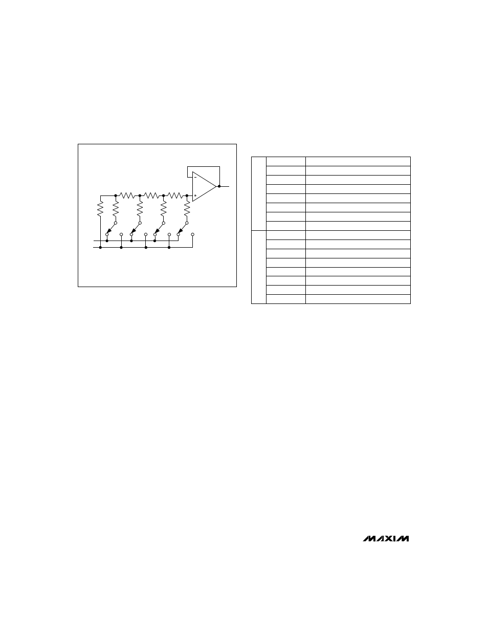
Figure 1. DAC Simplified Circuit Diagram
2R
2R
2R
2R
2R
R
R
R
REF
GND
OUT
SHOWN FOR ALL 1s ON DAC
Table 1. Input Shift Register
*
*
Clocked in last.
**Clocked in first.
Uncommitted Bit 1
UB1**
Uncommitted Bit 2
UB2
Uncommitted Bit 3
UB3
Shut Down DAC B, Active High
SB
Shut Down DAC A, Active High
SA
Uncommitted Bit 4
UB4
Load Reg DAC B, Active High
LB
Load Reg DAC A, Active High
LA
DAC Data Bit 7 (MSB)
B7
DAC Data Bit 6
B6
DAC Data Bit 5
B5
DAC Data Bit 4
B4
DAC Data Bit 3
B3
DAC Data Bit 2
B2
DAC Data Bit 1
B1
DAC Data Bit 0 (LSB)
B0*
DATA BITS
CONTROL BITS
Serial Interface
An active-low chip select (
–
C
—
S
–
) enables the shift register
to receive data from the serial data input. Data is
clocked into the shift register on every rising edge of
the serial clock signal (SCLK). The clock frequency can
be as high as 5MHz.
Data is sent MSB first and can be transmitted in one 16-
bit word. The write cycle can be segmented when
–
C
—
S
–
is
kept active (low) to allow, for example, two 8-bit-wide
transfers. After clocking all 16 bits into the input shift
register, the rising edge of
–
C
—
S
–
updates the DAC outputs
and the shutdown status. Because of their single
buffered structure, DACs cannot be simultaneously
updated to different digital values.
Serial-Input Data Format and Control Codes
Table 2 lists the serial-input data format. The 16-bit
input word consists of an 8-bit control byte and an 8-bit
data byte. The 8-bit control byte is not decoded inter-
nally. Every control bit performs one function. Data is
clocked in starting with UB1 (Uncommitted Bit), fol-
lowed by the remaining control bits and the data byte.
The LSB of the data byte (B0) is the last bit clocked into
the shift register (Figure 2).
Table 3 is an example of a 16-bit input word. It per-
forms the following functions:
• 80hex (128 decimal) loaded into DAC registers
A and B.
• DAC A and DAC B are active.