Electrical characteristics (continued) – Rainbow Electronics MAX522 User Manual
Page 3
MAX522
Dual, 8-Bit, Voltage-Output
Serial DAC in 8-Pin SO Package
_______________________________________________________________________________________
3
Note 2:
Reduced digital code range (code 24 through code 232) is due to swing limitations of the output amplifiers. See
Typical
Operating Characteristics
.
Note 3:
Reference input resistance is code dependent. The lowest input resistance occurs at code 55hex. Refer to the
Reference
Input
section in the
Detailed Description
.
Note 4:
Guaranteed by design. Not production tested.
Note 5:
Input capacitance is code dependent. The highest capacitance occurs at code 00hex.
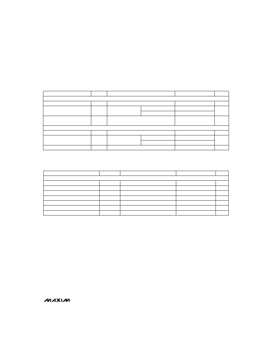
CONDITIONS
UNITS
MIN
TYP
MAX
SYMBOL
PARAMETER
ELECTRICAL CHARACTERISTICS (continued)
(V
DD
= +2.7V to +5.5V, REF = V
DD
, T
A
= T
MIN
to T
MAX
, unless otherwise noted. Typical values are at T
A
= +25°C.)
Voltage-Output Slew Rate
SR
C
L
= 0.1µF (DAC A), C
L
= 0.01µF (DAC B)
0.1
V/µs
70
Voltage-Output Settling Time
To ±
1
⁄
2
LSB
µs
Digital Feedthrough
and Crosstalk
All 0s to all 1s
10
nV-s
Supply Voltage Range
V
DD
2.7
5.5
V
Shutdown Supply Current
V
DD
= 5.5V
0.1
µA
C
L
= 0.1µF (DAC A)
C
L
= 0.01µF (DAC B)
70
Supply Current
I
DD
All inputs = 0V
1.3
2.8
mA
0.9
2.5
DYNAMIC PERFORMANCE
POWER SUPPLIES
V
DD
= 5.5V
V
DD
= 3.6V
TIMING CHARACTERISTICS (Note 4)
(V
DD
= +2.7V to +5.5V, T
A
= T
MIN
to T
MAX
, unless otherwise noted.)
CONDITIONS
ns
200
t
CSPWH
–
C
—
S
–
Pulse Width High
ns
100
t
CL
SCLK Pulse Width Low
ns
100
t
CH
SCLK Pulse Width High
ns
50
t
DH
DIN to SCLK Rise Hold Time
ns
50
t
DS
DIN to SCLK Rise Setup Time
UNITS
MIN
TYP
MAX
SYMBOL
PARAMETER
ns
150
t
CSS
–
C
—
S
–
Fall to SCLK Rise Setup Time
ns
150
t
CSH
SCLK Rise to
–
C
—
S
–
Rise Setup Time
SERIAL INTERFACE TIMING