Power-up sequencing and fault protection, Vcom buffer startup – Rainbow Electronics MAX1885 User Manual
Page 34
MAX1778/MAX1880–MAX1885
Quad-Output TFT LCD DC-DC
Converters with Buffer
34
______________________________________________________________________________________
converter steps up the input voltage so that the linear
regulator will not drop out. Therefore, to guarantee that
the external pass transistor does not saturate, the step-
up converter’s output voltage must be set above the lin-
ear regulator’s output voltage plus the transistor’s
saturation rating (V
MAIN
≥ V
LDO
+ V
SAT
).
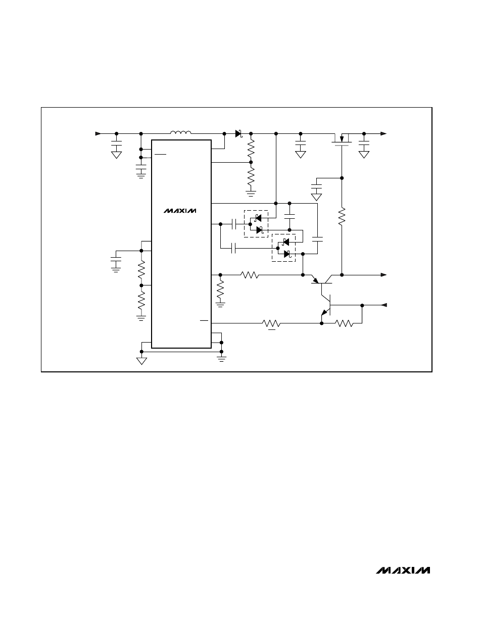
Power-Up Sequencing and Fault Protection
The MAX1778/MAX1880–MAX1885’s fault protection
cannot be activated until the power-up sequence is
successfully completed and the power ready output
goes low. Therefore, faults on the main output or posi-
tive charge-pump output could damage the controller
or external components. Additional fault protection may
be added as shown in Figure 10. The external MOSFET
and PNP transistor isolate the positive outputs during
startup. When the controller finishes the power-up
sequence, the power-ready output goes low, turning on
the PNP transistor. Any fault on the positive charge-
pump output will pull down the charge pump’s output
voltage and trigger the fault protection; otherwise, the
MOSFET’s gate slow charges. Once the MOSFET turns
on, any faults on the main step-up converter’s output
will pull down the main output voltage and trigger the
fault protection.
VCOM Buffer Startup
The VCOM buffer does not include soft-start. Therefore,
once the VCOM buffer turns on, it draws high surge
currents while charging the output capacitance. In
some applications, the buffer’s high startup surge
current could potentially trip the fault detection circuit,
forcing the controller to shut down. In these cases,
adding a soft-start resistive divider between SUPB and
BUFOUT reduces the startup surge current and voltage
drops associated with this load (Figure 11), as shown in
IN
SYSTEM
POSITIVE
V
POS(SYS)
= 20V
STARTUP
POSITIVE
V
POS(START)
= 20V
INPUT
V
IN
= 3.3V
SHDN
SUPP
LX
L1
6.8
µH
INPUT
V
IN
= 3.3V
C1
0.22
µF
C5
1.0
µF
C7
1.0
µF
Q2
Q3
C
OUT
(2) 3.3
µF
C4
0.1
µF
C
IN
4.7
µF
R10
100k
Ω
R
RDY
5.1k
Ω
R1
274k
Ω
R2
49.9k
Ω
R7
10k
Ω
FB
RDY
FBP
DRVP
GND
TGND
REF
FLTSET
INTG
PGND
C
REF
0.22
µF
MAX1778
C8
3.3
µF
SYSTEM MAIN
V
MAIN(SYS)
= 8V
STARTUP MAIN
V
MAIN(START)
= 8V
C10
0.1
µF
C6
0.1
µF
R8
100k
Ω
R3
750k
Ω
R4
49.9k
Ω
R9
30k
Ω
Figure 10. Power-Up Sequencing and Fault Protection;