Applications information, Low-profile components, Desktop monitors – Rainbow Electronics MAX1885 User Manual
Page 33: Input voltage above and below the output voltage

MAX1778/MAX1880–MAX1885
Quad-Output TFT LCD DC-DC
Converters with Buffer
______________________________________________________________________________________
33
Applications Information
Low-Profile Components
Notebook applications generally require low-profile
components, potentially limiting the circuit’s perfor-
mance. For example, low-profile inductors typically
have lower saturation ratings and more series resis-
tance, limiting output current and efficiency. Low-profile
capacitors have lower voltage ratings for a given
capacitance value, so 3.3µF low-profile capacitors with
voltage ratings greater than 10V were not available at
the time of publication.
Desktop Monitors
Monitor applications do not have the same component
height restrictions associated with laptops, allowing
more flexibility in component selection (Figure 8).
Larger output capacitors with higher voltage ratings
allow configurations with output voltages above 10V.
Additionally, physically larger inductors with less series
resistance and higher saturation ratings provide more
output current and higher efficiency.
Input Voltage Above and
Below the Output Voltage
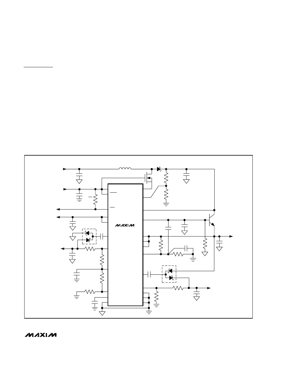
Combining the step-up converter and linear regulator
as shown in Figure 9 provides output voltage regulation
above and below the input voltage. Supplied by the
step-up converter, the linear regulator output provides
a constant output voltage (V
LDO
). When the input volt-
age exceeds the main step-up converter’s nominal out-
put voltage, the controller stops switching but the linear
regulator maintains the output voltage. When the input
voltage drops below the output voltage, the step-up
IN
BUFFER OUTPUT
V
BUFOUT
= V
SUPB
/2
POSITIVE
V
POS
= 24V
SHDN
RDY
BUF-
BUFOUT
SUPN
SUPP
LX
L1
6.8
µH
POWER INPUT
V
BATT
= 10V TO 15V
INPUT
V
IN
= 3.3V TO 5V
C1
0.1
µF
C
LDO
(2) 3.3
µF
C6
0.1
µF
C7
0.1
µF
C3
1.0
µF
C
BUF
1.0
µF
C
INTG
470pF
C2
0.1
µF
C
OUT
(3) 3.3
µF
C4
0.1
µF
C
IN
4.7
µF
C
LDOOUT
3.3
µF
R
RDY
100k
Ω
R10
100k
Ω
R5
475k
Ω
R3
909k
Ω
R8
49.9k
Ω
R1
511k
Ω
R2
49.9k
Ω
R4
49.9k
Ω
R7
470k
Ω
R6
49.9k
Ω
R9
6.8k
Ω
NEGATIVE
V
NEG
= -12V
TO LOGIC
FB
FBL
SUPL
LDOOUT
BUF+
FBP
DRVP
GND
TGND
FBN
DRVN
REF
FLTSET
INTG
PGND
SUPB
C
REF
0.22
µF
MAX1778
LDO
V
LDO
= 13V
Q1
C5
1.0
µF
R9
30k
Ω
Figure 9. Input Voltage Above and Below the Output Voltage
