Rainbow Electronics MAX1885 User Manual
Page 32

MAX1778/MAX1880–MAX1885
Quad-Output TFT LCD DC-DC
Converters with Buffer
32
______________________________________________________________________________________
regulator and charge-pump power ground plane,
and the inner layer should contain the analog
ground plane and power-ground plane/path for the
V
COM
buffer and LDO. Connect all three ground
planes together at one place near the PGND pin.
3) Locate all feedback resistive-dividers as close to
their respective feedback pins as possible. The
voltage-divider’s center trace should be kept short.
Avoid running any feedback trace near the LX
switching node or the charge-pump drivers. The
resistive-dividers’ ground connections should be to
analog ground (GND).
4) When using multilayer boards, separate the top sig-
nal layer and bottom signal layer with a ground
plane between to eliminate capacitive coupling
between fast-charging nodes on the top layer and
high-impedance nodes on the bottom layer. The
fast-charging nodes, such as the LX and charge-
pump driver nodes, should not have any other
traces or ground planes near by.
5) Keep the charge-pump circuitry as close to the IC
as possible, using wide traces and avoiding vias
when possible. Place 0.1µF ceramic bypass
capacitors near the charge-pump input pins (SUPP
and SUPN) to the PGND pin.
6) To maximize output power and efficiency and mini-
mize output ripple voltage, use extra wide, power
ground traces, and solder the IC’s power ground
pin directly to it.
Refer to the MAX1778/MAX1880-MAX1885 evaluation
kit for an example of proper board layout.
IN
BUFFER OUTPUT
V
BUFOUT
= V
SUPB
/2
POSITIVE
V
POS
= 20V
SHDN
RDY
SUPL
LDOOUT
SUPN
SUPP
DRVP
FBP
LX
L1
10
µH
INPUT
V
IN
= 5V
C1
0.22
µF
C6
1
µF
C6
0.01
µF
C7
0.01
µF
C3
1.0
µF
C
REF
0.22
µF
C2
0.1
µF
C
BUF
1.0
µF
C5
1.0
µF
C
COMP
470pF
C
OUT
(2) 10
µF
C4
0.1
µF
C
IN
(2) 4.7
µF
C
LDOOUT
4.7
µF
R
RDY
100k
Ω
R8
1.5k
Ω
R8
10k
Ω
R5
316k
Ω
R9
30k
Ω
R3
750k
Ω
R4
49.9k
Ω
R1
86.6k
Ω
R2
10k
Ω
R
COMP
4.7k
Ω
R10
100k
Ω
R6
49.9k
Ω
R7
16.4k
Ω
NEGATIVE
V
NEG
= -8V
TO LOGIC
FB
BUFOUT
BUF-
BUF+
FLTSET
GND
TGND
FBL
DRVN
FBN
REF
INTG
PGND
SUPB
MAX1778
LDO
V
LDO
= 3.3V
Q1
REF
MAIN
V
MAIN
= 12V
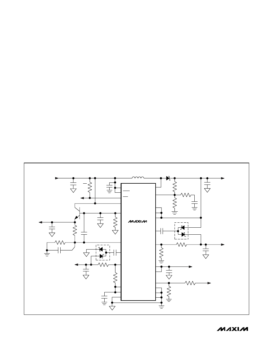
Figure 8. 5V Input Monitor Application
