Detailed description – Rainbow Electronics MAX1885 User Manual
Page 19

MAX1778/MAX1880–MAX1885
Quad-Output TFT LCD DC-DC
Converters with Buffer
______________________________________________________________________________________
19
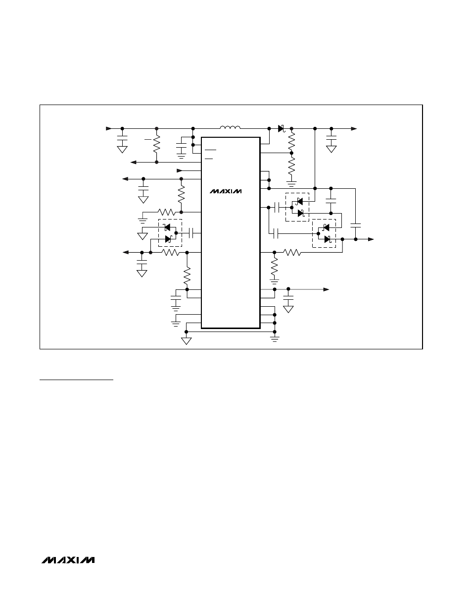
Detailed Description
The MAX1778/MAX1880–MAX1885 are highly efficient
multiple-output power supplies for thin-film transistor
(TFT) liquid crystal display (LCD) applications. The
devices contain one high-power step-up converter, two
low-power charge pumps, an operational transconduc-
tance amplifier (V
COM
buffer), and a low-dropout linear
regulator. The primary step-up converter uses an inter-
nal N-channel MOSFET to provide maximum efficiency
and to minimize the number of external components.
The output voltage of the main step-up converter
(V
MAIN
) can be set from V
IN
to 13V with external resis-
tors.
The dual charge pumps (MAX1778/MAX1880/
MAX1881/MAX1882 only) independently regulate a
positive output (V
POS
) and a negative output (V
NEG
).
These low-power outputs use external diode and
capacitor stages (as many stages as required) to regu-
late output voltages from -40V to +40V. A unique
control scheme minimizes output ripple as well as
capacitor sizes for both charge pumps.
A resistor-programmable 40mA linear regulator
(MAX1778/MAX1881/MAX1883/MAX1884 only) can
provide preregulation or postregulation for any of the
supplies. For higher current applications, an external
transistor can be added.
Additionally, the V
COM
buffer provides a high current
output that is ideal for driving capacitive loads, such as
the backplane of a TFT LCD panel. The positive feed-
back input features dual mode operation, allowing this
input to be connected to an internal 50% resistive-
divider between the buffer’s supply voltage and
ground, or externally adjusted for other voltages.
Also included in the MAX1778/MAX1880–MAX1885 is a
precision 1.25V reference that sources up to 50µA,
logic shutdown, soft-start, power-up sequencing,
adjustable fault detection, thermal shutdown, and an
active-low, open-drain ready output.
IN
BUFFER OUTPUT
V
BUFOUT
= V
SUPB
/2
POSITIVE
V
POS
= 20V
C
BUF
1.0
µF
C
LDO
4.7
µF
C
REF
0.22
µF
C7
1.0
µF
C5
1.0
µF
C4
0.1
µF
L1
6.8
µH
C4
0.1
µF
C2
0.1
µF
C1
0.22
µF
C
IN
4.7
µF
SHDN
RDY
SUPL
LDOOUT
SUPN
SUPP
DRVP
FBP
R3
750k
Ω
R5
200k
Ω
R7
150k
Ω
R4
49.9k
Ω
R6
49.9k
Ω
R8
49.9k
Ω
R2
49.9k
Ω
R2
274k
Ω
LX
INPUT
V
IN
= 3.3V
LDO
V
LDOOUT
= 5V
NEGATIVE
V
NEG
= -5V
TO LOGIC
FB
BUFOUT
BUF-
BUF+
GND
TGND
FBL
DRVN
FBN
REF
FLTSET
INTG
PGND
SUPB
MAX1778
MAIN
V
MAIN
= 8V
MAIN
(8V)
C
OUT
(2) 4.7
µF
C3
1.0
µF
R
RDY
100k
Ω
Figure 1. Typical Application Circuit
