Detailed description, Layout issues, Prototype chip installation – Rainbow Electronics MAX2374 User Manual
Page 6: Ucsp reliability, Marking information, Pin configuration, Chip information

MAX2374
SiGe, Variable IIP3, Low-Noise Amplifier
in UCSP Package
6
_______________________________________________________________________________________
Detailed Description
The MAX2374 SiGe LNA is packaged in a UCSP pack-
age in order to deliver high gain, high linearity, and low
noise in the smallest package possible. The special
feature of this LNA is that its linearity is adjusted by an
external resistor, R
BIAS
. The LNA has two digitally con-
trollable gain modes to increase system dynamic
range. Digital high at GAIN selects the high-gain mode,
and digital low selects the low-gain mode.
Adjust the LNA bias current to control the amplifier’s lin-
earity. The resistor R
BIAS
connected between BIAS and
V
CC
controls the LNA current. The amplifier’s linearity is
directly related to the operating current. Increasing the
bias current of the LNA increases the IIP3. V
BIAS
is
approximately constant at V
CC
- 1.16V. Connecting a
resistor from BIAS to V
CC
results in a supply current
that can be calculated as follows:
V
CC
= (High Gain) ~
– (150 - 1.16V) / R
BIAS
I
BIAS
can be set by a fixed resistor to V
CC
as described
above, or it can be generated with a switched network.
To operate the LNA in high-gain/high-linearity mode,
set R
BIAS
= 20k
Ω and drive GAIN high. Do this in the
presence of a transmit signal to minimize cross-modu-
lation. To operate the LNA in low-gain/low-linearity
mode, set R
BIAS
= 43k
Ω and drive GAIN high. This
mode draws less current and should be used in the
absence of a transmit signal (paging mode). Shutdown
of the IC is accomplished by switching R
BIAS
to open
circuit.
Layout Issues
Design the layout for the IC to be as compact as possi-
ble to minimize the parasitics. The chip-scale IC pack-
age uses a bump pitch of 0.5mm (19.7mil) and bump
diameter of 0.3mm (~12mil). Therefore, lay out the sol-
der-pad spacing on 0.5mm (19.7mil) centers, using a
pad size of 0.25mm (~10mil) and a solder mask open-
ing of 0.33mm (13mil). Round or square pads are per-
missible. Connect multiple vias from the ground plane
as close to the ground pins as possible.
Install capacitors as close as possible to the IC supply
voltage pin and supply end of the series inductor.
Place the ground end of these capacitors near the IC
GND pins to provide a low-impedance return path for
the signal current.
Prototype Chip Installation
Alignment keys on the PC board around the area where
the chip is located will be helpful in the prototype
assembly process. It is better to align the chip on the
board before any other components are placed, and
then place the board on a hot plate or hot surface until
the solder starts melting. Remove the board from the
hot plate without disturbing the position of the chip, and
let it cool down to room temperature before processing
the board further.
UCSP Reliability
The ultra-chip-scale package (UCSP) represents a
unique packaging form factor that may not perform
equally well as a packaged product through traditional
mechanical reliability tests. UCSP reliability is integrally
linked to the user’s assembly methods, circuit board
material, and usage environment. The user should
closely review these areas when considering use of a
UCSP package.
Performance through operating-life test and moisture
resistance remains uncompromised as it is primarily
determined by the wafer-fabrication process.
Mechanical stress performance is a greater considera-
tion for UCSP packages. UCSPs are attached through
direct solder contact to the user’s PC board, foregoing
the inherent stress relief of a packaged product lead
frame. Solder joint contact integrity must be consid-
ered. Comprehensive reliability tests have been per-
formed and are available upon request. In conclusion,
the UCSP performs reliably through environmental
stresses.
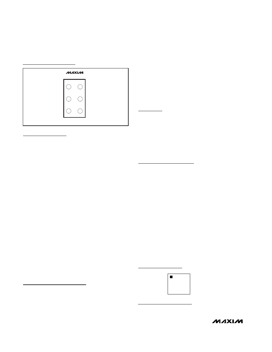
Marking Information
MAX2374
UCSP
TOP VIEW
(BUMPS ON BOTTOM)
BIAS
B3
V
CC
B2
LNAOUT
B1
LNAIN
GAIN
A3
GND
A2
A1
Pin Configuration
A A A
A A A
ORIENTATION
PRODUCT ID CODE
LOT CODE
TRANSISTOR COUNT: 296
Chip Information
