Detailed description, Pin description (continued) – Rainbow Electronics MAX1195 User Manual
Page 11
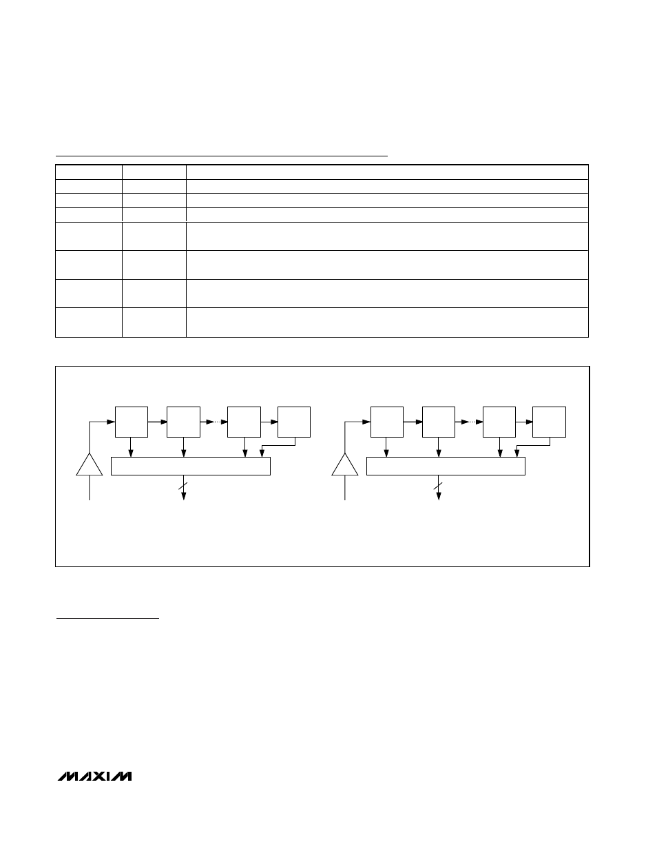
Detailed Description
The MAX1195 uses a seven-stage, fully differential,
pipelined architecture (Figure 1) that allows for high-
speed conversion while minimizing power consump-
tion. Samples taken at the inputs move progressively
through the pipeline stages every half-clock cycle.
Including the delay through the output latch, the total
clock-cycle latency is five clock cycles.
Flash ADCs convert the held input voltages into a digi-
tal code. Internal MDACs convert the digitized results
back into analog voltages, which are then subtracted
from the original held input signals. The resulting error
signals are then multiplied by two, and the residues are
passed along to the next pipeline stages where the
process is repeated until the signals have been
processed by all seven stages.
Input Track-and-Hold Circuits
Figure 2 displays a simplified functional diagram of the
input T/H circuits in both track and hold mode. In track
mode, switches S1, S2a, S2b, S4a, S4b, S5a, and S5b
are closed. The fully differential circuits sample the
input signals onto the two capacitors (C2a and C2b)
through switches S4a and S4b. S2a and S2b set the
common mode for the amplifier input, and open simul-
MAX1195
Dual, 8-Bit, 40Msps, 3V, Low-Power ADC with
Internal Reference and Parallel Outputs
______________________________________________________________________________________
11
Pin Description (continued)
PIN
NAME
FUNCTION
42
D5A
Three-State Digital Output, Bit 5, Channel A
43
D6A
Three-State Digital Output, Bit 6, Channel A
44
D7A
Three-State Digital Output, Bit 7 (MSB), Channel A
45
REFOUT
Internal Reference Voltage Output. May be connected to REFIN through a resistor or a resistor
divider.
46
REFIN
Reference Input. V
REFIN
= 2 x (V
REFP
– V
REFN
).
Bypass to GND with a > 0.1µF capacitor.
47
REFP
Positive Reference I/O. Conversion range is
±(V
REFP
– V
REFN
).
Bypass to GND with a > 0.1µF capacitor.
48
REFN
Negative Reference I/O. Conversion range is
±(V
REFP
– V
REFN
).
Bypass to GND with a > 0.1µF capacitor.
8
V
INA
STAGE 1
STAGE 2
D7A–D0A
V
INA
= INPUT VOLTAGE BETWEEN INA+ AND INA- (DIFFERENTIAL OR SINGLE ENDED)
V
INB
= INPUT VOLTAGE BETWEEN INB+ AND INB- (DIFFERENTIAL OR SINGLE ENDED)
DIGITAL ALIGNMENT LOGIC
STAGE 6
STAGE 7
2-BIT FLASH
ADC
T/H
8
V
INB
STAGE 1
STAGE 2
D7B–D0B
DIGITAL ALIGNMENT LOGIC
STAGE 6
STAGE 7
2-BIT FLASH
ADC
T/H
Figure 1. Pipelined Architecture—Stage Blocks