Table 1. output voltage selection – Rainbow Electronics MAX1623 User Manual
Page 8

MAX1623
3A, Low-Voltage, Step-Down Regulator with
Synchronous Rectification and Internal Switches
8
_______________________________________________________________________________________
Setting the AC Loop Gain
The internal integrator amplifier effectively eliminates any
long-term error within the time constant set by the G
m
of
the transconductance amplifier and the capacitor con-
nected to COMP. However, there remains a short-term
load-regulation error in response to load current
changes. Proper FBSEL connection selects the relative
level of current feedback to voltage feedback, which
results in an AC load-regulation error of either 1% or 2%
of the output voltage (Table 1). The 2% setting is auto-
matically selected in preset output voltage mode (FBSEL
connected to V
CC
or unconnected). This gain setting
minimizes the size and cost of the output filter capacitor
required. For extremely tight specifications that cannot
tolerate 2% short-term errors, connect FBSEL to ground
(adjustable mode) for 1% AC load regulation (see the
Input and Output Filter Capacitors (C1, C2) section).
Synchronous Rectification
Synchronous rectification improves efficiency by 3% to
5% at heavy loads when compared to a conventional
Schottky rectifier. To prevent cross-conduction or “shoot-
through,” the synchronous rectifier turns on following a
short delay (dead time) after the P-channel power MOS-
FET turns off. In discontinuous (light-load) mode, the syn-
chronous rectifier switch turns off as the inductor current
approaches zero. The synchronous rectifier works under
all operating conditions, including Idle Mode.
Integrator Amplifier (COMP)
An internal transconductance amplifier fine tunes the
output DC accuracy. The transconductance amplifier is
compensated at COMP. A capacitor from COMP to
ground determines the gain-bandwidth product and the
overall loop response. This integrator effectively elimi-
nates any long-term error within the time constant set
by the G
m
of the transconductance amplifier and the
capacitor connected to COMP.
For stability, choose COMP as follows:
where G
m
= 9.1µS.
C
G
R
C
4
COMP
m
LOAD
OUT
≥
Ч
Ч
AC LOAD
REGULATION (%)
OUTPUT
VOLTAGE (V)
IN
2
2.525
Unconnected
2
3.33
FBSEL PIN
GND
1
Adjustable
V
REF
2
Adjustable
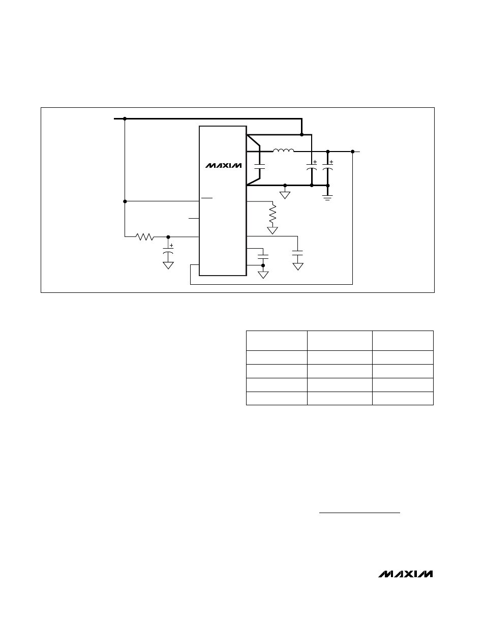
Figure 2. Standard 3.3V/3A Application Circuit
MAX1623
3.3V OUTPUT
INPUT
4.5V TO 5.5V
0.1
µF
4.7
µF
470pF
LX
IN
PGND
V
CC
COMP
REF
GND
10
µF
C1
220
µF
C2
330
µF
4.7
µH
10
Ω
110k
FBSEL
TOFF
FB
SHDN
NOTE: HEAVY LINES
DENOTE HIGH SWITCHING
CURRENT PATHS.
Table 1. Output Voltage Selection
