Rainbow Electronics MAX924 User Manual
Page 9

about 2.2V, although the comparators will continue to
operate with a total supply voltage as low as 1V. While
the MAX924 has comparators that may be used at
supply voltages below 2V, the MAX921, MAX922, and
MAX923 may not be used with supply voltages sig-
nificantly below 2.5V.
At low supply voltages, the comparators’ output drive is
reduced and the propagation delay increases (see
Typical Operating Characteristics). The useful input
voltage range extends from the negative supply to a
little under 1V below the positive supply, which is
slightly closer to the positive rail than the device
operating from higher supply voltages. Test your
prototype over the full temperature and supply-voltage
range if operation below 2.5V is anticipated.
Comparator Output
With 100mV of overdrive, propagation delay is typically
3µs. The
Typical Operating Characteristics show the
propagation delay for various overdrive levels.
The MAX921 and MAX924 output swings from V+ to
GND, so TTL compatibility is assured by using a +5V
±10% supply. The negative supply does not affect the
output swing, and can range from 0V to -5V ±10%.
The MAX922 and MAX923 have no GND pin, and their
outputs swing from V+ to V-. Connect V- to ground and
V+ to a +5V supply to achieve TTL compatibility.
The MAX921–MAX924’s unique design achieves an
output source current of more than 40mA and a sink
current of over 5mA, while keeping quiescent currents in
the microampere range. The output can source 100mA
(at V+ = 5V) for short pulses, as long as the package's
maximum power dissipation is not exceeded. The
output stage does not generate crowbar switching
currents during transitions, which minimizes feedback
through the supplies and helps ensure stability without
bypassing.
Voltage Reference
The internal bandgap voltage reference has an output
of 1.182V above V-. Note that the REF voltage is
referenced to V-, not to GND. Its accuracy is ±1% in
the range 0°C to +70°C. The REF output is typically
capable of sourcing 15µA and sinking 8µA. Do not
bypass the REF output.
Noise Considerations
Although the comparators have a very high gain, useful
gain is limited by noise. This is shown in the Transfer
Function graph (see
Typical Operating Characteristics).
As the input voltage approaches the comparator's
offset, the output begins to bounce back and forth; this
peaks when V
IN
= V
OS
. (The lowpass filter shown on
the graph averages out the bouncing, making the
transfer function easy to observe.) Consequently, the
comparator has an effective wideband peak-to-peak
noise of around 0.3mV. The voltage reference has
peak-to peak noise approaching 1mV. Thus, when a
MAX921–MAX924
Ultra Low-Power,
Single/Dual-Supply Comparators
_______________________________________________________________________________________
9
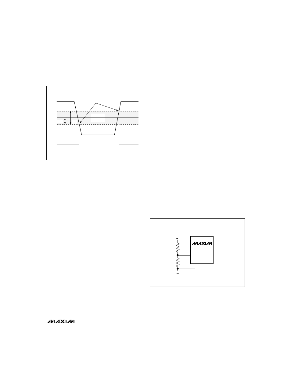
THRESHOLDS
OUT
IN-
IN+
V
HB
HYSTERESIS
BAND
VREF - VHYST
Figure 2. Threshold Hysteresis Band
7
2
5
6
HYST
REF
V-
V+
R1
R2
MAX921
MAX923
2.5V TO 11V
I
REF
Figure 3. Programming the HYST Pin
