Typical applications – Rainbow Electronics MAX924 User Manual
Page 11

6. Verify the threshold voltages with these formulas:
Board Layout and Bypassing
Power-supply bypass capacitors are not needed if the
supply impedance is low, but 100nF bypass capacitors
should be used when the supply impedance is high or
when the supply leads are long. Minimize signal lead
lengths to reduce stray capacitance between the input
and output that might cause instability. Do not bypass
the reference output.
_______________Typical Applications
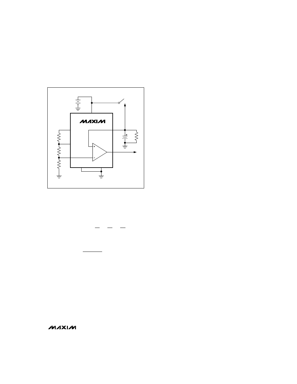
Auto-Off Power Source
Figure 5 shows the schematic for a 40mA power supply
that has a timed auto power-off function. The
comparator output is the switched power-supply
output. With a 10mA load, it typically provides a
voltage of (V
BATT
– 0.12V), but draws only 3.5µA
quiescent current. This circuit takes advantage of the
four key features of the MAX921: 2.5µA supply current,
an internal reference, hysteresis, and high current
output. Using the component values shown, the three-
resistor voltage divider programs the maximum ±50mV
of hysteresis and sets the IN- voltage at 100mV. This
gives an IN+ trip threshold of approximately 50mV for
IN+ falling.
The RC time constant determines the maximum power-
on time of the OUT pin before power-down occurs.
This period can be approximated by:
R x C x 4.6sec
For example: 2M
Ω
x 10µF x 4.6 = 92sec. The actual
time will vary with both the leakage current of the
capacitor and the voltage applied to the circuit.
Window Detector
The MAX923 is ideal for making window detectors
(undervoltage/overvoltage detectors). The schematic
is shown in Figure 6, with component values selected
for an 4.5V undervoltage threshold, and a 5.5V
overvoltage threshold. Choose different thresholds by
changing the values of R1, R2, and R3. To prevent
chatter at the output when the supply voltage is close
to a threshold, hysteresis has been added using R4
and R5. OUTA provides an active-low undervoltage
indication, and OUTB gives an active-low overvoltage
indication. ANDing the two outputs provides an active-
high, power-good signal.
The design procedure is as follows:
1. Choose the required hysteresis level and calculate
values for R4 and R5 according to the formulas in
the
Hysteresis (MAX921/MAX923) section. In this
example, ±5mV of hysteresis has been added
at the
comparator input (V
H
= V
HB
/2). This means that the
hysteresis apparent at V
IN
will be larger because of
the input resistor divider.
V rising :
V
V
R1
1
R1
1
R2
1
R3
V falling :
V
V
R1
V
R3
IN
THR
REF
IN
THF
THR
=
Ч
Ч
+
+
=
−
Ч
+
(
)
MAX921–MAX924
Ultra Low-Power,
Single/Dual-Supply Comparators
______________________________________________________________________________________
11
MAX921
OUT
IN-
HYST
REF
V-
GND
IN+
V+
VBATT -0.15V
10mA
2
1
4
5
6
8
3
100k
1.1M
47k
4.5V TO 6.0V
MOMENTARY
SWITCH
7
R
C
Figure 5. Auto-off power switch operates on 2.5µA quiescent
current.
