Max1208, Bit, 80msps, 3.3v adc – Rainbow Electronics MAX1208 User Manual
Page 16

MAX1208
All three modes of reference operation require the
same bypass capacitor combinations. Bypass COM
with a 2.2µF capacitor to GND. Bypass REFP and
REFN each with a 0.1µF capacitor to GND. Bypass
REFP to REFN with a 1µF capacitor in parallel with a
10µF capacitor. Place the 1µF capacitor as close to
the device as possible on the same side of the PC
board. Bypass REFIN and REFOUT to GND with a
0.1µF capacitor.
For detailed circuit suggestions, see Figures 13 and 14.
Clock Input and Clock Control Lines
(CLKP, CLKN, CLKTYP)
The MAX1208 accepts both differential and single-
ended clock inputs. For single-ended clock-input oper-
ation, connect CLKTYP to GND, CLKN to GND, and
drive CLKP with the external single-ended clock signal.
For differential clock-input operation, connect CLKTYP
to OV
DD
or V
DD
, and drive CLKP and CLKN with the
external differential clock signal. To reduce clock jitter,
the external single-ended clock must have sharp falling
edges. Consider the clock input as an analog input and
route it away from any other analog inputs and digital
signal lines.
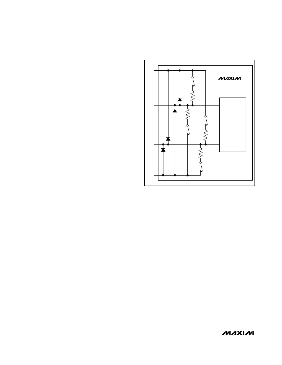
CLKP and CLKN are high impedance when the
MAX1208 is powered down (Figure 5).
Low clock jitter is required for the specified SNR perfor-
mance of the MAX1208. Analog input sampling occurs
on the falling edge of the clock signal, requiring this
edge to have the lowest possible jitter. Jitter limits the
maximum SNR performance of any ADC according to
the following relationship:
where f
IN
represents the analog input frequency and t
J
is the total system clock jitter. Clock jitter is especially
critical for undersampling applications. For example,
assuming that clock jitter is the only noise source, to
obtain the specified 68.2dB of SNR with an input fre-
quency of 32.5MHz, the system must have less than
1.9ps of clock jitter.
Clock Duty-Cycle Equalizer (DCE)
Enable the MAX1208 clock duty-cycle equalizer by
connecting DCE to OV
DD
or V
DD
. Disable the MAX1208
clock duty-cycle equalizer by connecting DCE to GND.
The clock duty-cycle equalizer uses a delay-locked
loop (DLL) to create internal timing signals that are
duty-cycle independent. Due to this DLL, the MAX1208
requires approximately 100 clock cycles to acquire and
lock to new clock frequencies.
Disabling the clock duty-cycle equalizer reduces the
analog supply current by 1.5mA.
System Timing Requirements
Figure 6 shows the relationship between the clock, ana-
log inputs, DAV indicator, DOR indicator, and the result-
ing output data. The analog input is sampled on the
falling edge of the clock signal and the resulting data
appears at the digital outputs 8.5 clock cycles later.
The DAV indicator is synchronized with the digital out-
put and optimized for use in latching data into digital
back-end circuitry. Alternatively, digital back-end cir-
cuitry can be latched with the rising edge of the con-
version clock (CLKP-CLKN).
SNR
f
t
IN
J
log
=
Ч
Ч π
×
20
1
2
12-Bit, 80Msps, 3.3V ADC
16
______________________________________________________________________________________
MAX1208
CLKP
CLKN
V
DD
GND
10k
Ω
10k
Ω
10k
Ω
10k
Ω
DUTY-CYCLE
EQUALIZER
SWITCHES S
1_
AND S
2_
ARE OPEN
DURING POWER-DOWN, MAKING
CLKP AND CLKN HIGH IMPEDANCE.
SWITCHES S
2_
ARE OPEN IN
SINGLE-ENDED CLOCK MODE.
S
1H
S
2H
S
1L
S
2L
Figure 5. Simplified Clock Input Circuit
