Functional description, 0 smbus, 1 addressing – Rainbow Electronics LM85 User Manual
Page 7: 0 fan register device set-up, Error(note 12), Note 13), Logic(note 14), Lm85

Note 12: TUE , total unadjusted error, includes ADC gain, offset, linearity and reference errors. TUE is defined as the "actual Vin" to achieve a given code transition
minus the "theoretical Vin" for the same code. Therefore, a positive error indicates that the input voltage is greater than the theoretical input voltage for a given code.
If the theoretical input voltage was applied to an LM85 that has positive error, the LM85’s reading would be less than the theoretical.
Note 13: This specification is provided only to indicate how often temperature and voltage data is updated. The LM85 can be read at any time without regard to
conversion state (and will yield last conversion result).
Note 14: Holding the SMBDAT and/or SMBCLK lines Low for a time interval greater than t
TIMEOUT
will reset the LM85’s SMBus state machine, therefore setting the
SMBDAT pin to a high impedance state.
Functional Description
1.0 SMBUS
The LM85 is compatible with devices that are compliant to the SMBus 2.0 specification. More information on this bus can be found
at: http://www.smbus.org/. Compatibility of SMBus2.0 to other buses is discuss in the SMBus 2.0 specification.
1.1 Addressing
LM85 is designed to be used primarily in desktop systems that require only one monitoring device.
If only one LM85 is used on the motherboard, the designer should be sure that the Address Enable/PWM3 pin is High during the
first SMBus communication addressing the LM85. Address Enable/PWM3 is an open drain I/O pin that at power-on defaults to
the input state. A maximum of 10k pull-up resistance is required to assure that the SMBus address of the device will be locked
at 010 1110b, which is the default address of the LM85.
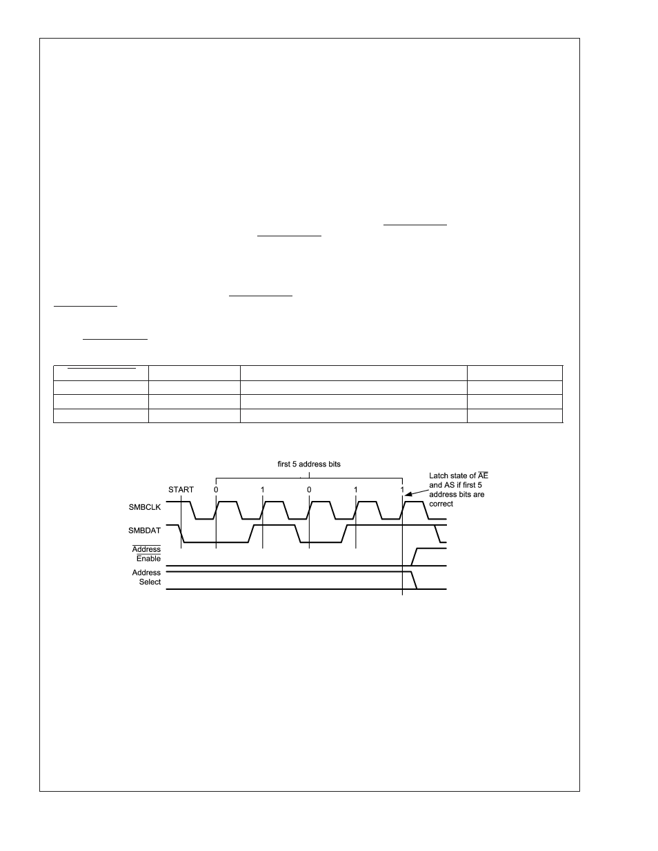
During the first SMBus communication TACH4 and PWM3 can be used to change the SMBus address of the LM85. to 0101101b
or 0101100b. LM85 address selection procedure:
A 10 k
Ω pull-down resistor to ground on the Address Enable/PWM3 pin is required. Upon power up, the LM85 will be placed into
Address Enable mode and assign itself an SMBus address according to the state of the Address Select input. The LM85 will latch
the address during the first valid SMBus transaction in which the first five bits of the targeted address match those of the LM85
address, 0 1011b. This feature eliminates the possibility of a glitch on the SMBus interfering with address selection. When the
PWM3/Address Enable pin is not used to change the SMBus address of the LM85, it will remain in a high state until the first
communication with the LM85. After the first SMBus transaction is completed PWM3 and TACH4 will return to normal operation.
Address Enable
Address Select
Board Implementation
SMBus Address
0
0
Pulled to ground through a 10 k
Ω resistor
010 1100b, 2Ch
0
1
Pulled to 3.3V or ground through a 10 k
Ω resistor
010 1101b, 2Dh
1
X
Pulled to 3.3V through a 10k
Ω resistor
010 1110b, 2Eh
In this way, up to three LM85 devices can exists on an SMBus at any time. Multiple LM85 devices can be used to monitor
additional processors and temperature zones.
20035304
2.0 FAN REGISTER DEVICE SET-UP
The BIOS will follow the following steps to configure the fan registers on the LM85. The registers corresponding to each function
are listed. All steps may not be necessary if default values are acceptable. Regardless of all changes made by the BIOS to the
fan limit and parameter registers during configuration, the LM85 will continue to operate based on default values until the START
bit (bit 0), in the Ready/Lock/Start/Override register (address 40h), is set. Once the fan mode is updated, by setting the START
bit to 1, the LM85 will operate using the values that were set by the BIOS in the fan control limit and parameter registers (adress
5Ch through 6Eh).
LM85
www.national.com
7
