Rainbow Electronics MAX747 User Manual
Page 9
MAX747
High-Efficiency PWM, Step-Down
P-Channel DC-DC Controller
_______________________________________________________________________________________
9
duty cycle) is 331mW. Metal film resistors are
recommended. Do not use wire-wound resistors because
their inductance will adversely affect circuit operation.
Determine the duty cycle for CCM from the following
equation:
where V
SW
is the voltage drop across the external P-
FET and sense resistor, and can be approximated as
(I
LOAD
)[R
DS(ON)
+ R
SENSE
].
Inductor Selection
Once the sense resistor value is determined, the
inductor is determined from the following equation. The
value of inductor L ensures proper slope
compensation. Continuing with the above example,
Although 38µH is the calculated value, the component
used may have a tolerance of ±30% or more. Make
sure the inductor’s saturation current rating (the current
at which the core begins to saturate and the
inductance starts to fall) exceeds the peak current set
by R
SENSE
.
Inductors with molypermalloy powder (MPP), Kool Mµ,
or ferrite are recommended. Inexpensive iron powder
core inductors are not suitable due to their increased
core losses. MPP and Kool Mµ cores have low
permeability, allowing larger currents.
For highest efficiency, use a coil with low DC
resistance. To minimize radiated noise, use a toroid,
pot core, or shielded coil.
External P-FET Selection
To ensure the external P-FET is fully on, use logic-level,
or low threshold P-FETs when the minimum input
voltage is less than 8V.
When selecting the P-FET, three important parameters
to note are total gate charge (Q
g
), on resistance
(R
DS(ON)
), and reverse transfer capacitance (C
RSS
).
Q
g
, the total gate charge, includes all capacitances
associated with charging the gate. Use the typical Q
g
value for best results; the maximum value is usually
overspecified since it is a guaranteed limit and not the
measured value. The typical total gate charge should
be
≤
50nC. Larger numbers mean that EXT may not be
able to adequately drive the gate. EXT sink/source
capability (I
EXT
) is typically 140mA.
There are two losses associated with the P-FET’s power
dissipation: I
2
R losses and switching losses. CCM
power dissipation (PD) is approximated by:
where the duty cycle is approximated by V
OUT
/V+, f
OSC
=
100kHz, and R
DS(ON)
and C
RSS
are given in the data
sheet of the chosen P-FET. In the equation, R
DS(ON)
is
assumed to be constant, but is actually a function of
temperature. Note that the equation does not account
for losses incurred by charging and discharging the
PD
Duty
Cycle
I
R
+
V +
C
I
f
I
PK
DS(ON)
2
RSS
PK
OSC
EXT
=
(
)
[
]
(
) ( ) ( )
2
L
(R
) (V
)
(V
) (f
)
(38m ) (5V)
(50mV) (100kHz)
38 H
SENSE
OUT(MAX)
RAMP(MAX)
OSC
=
=
Ω
=
µ
Duty cycle (%)
V
V
V
V
V
100%
OUT
DIODE
SW
DIODE
=
+
+ −
+
(
)
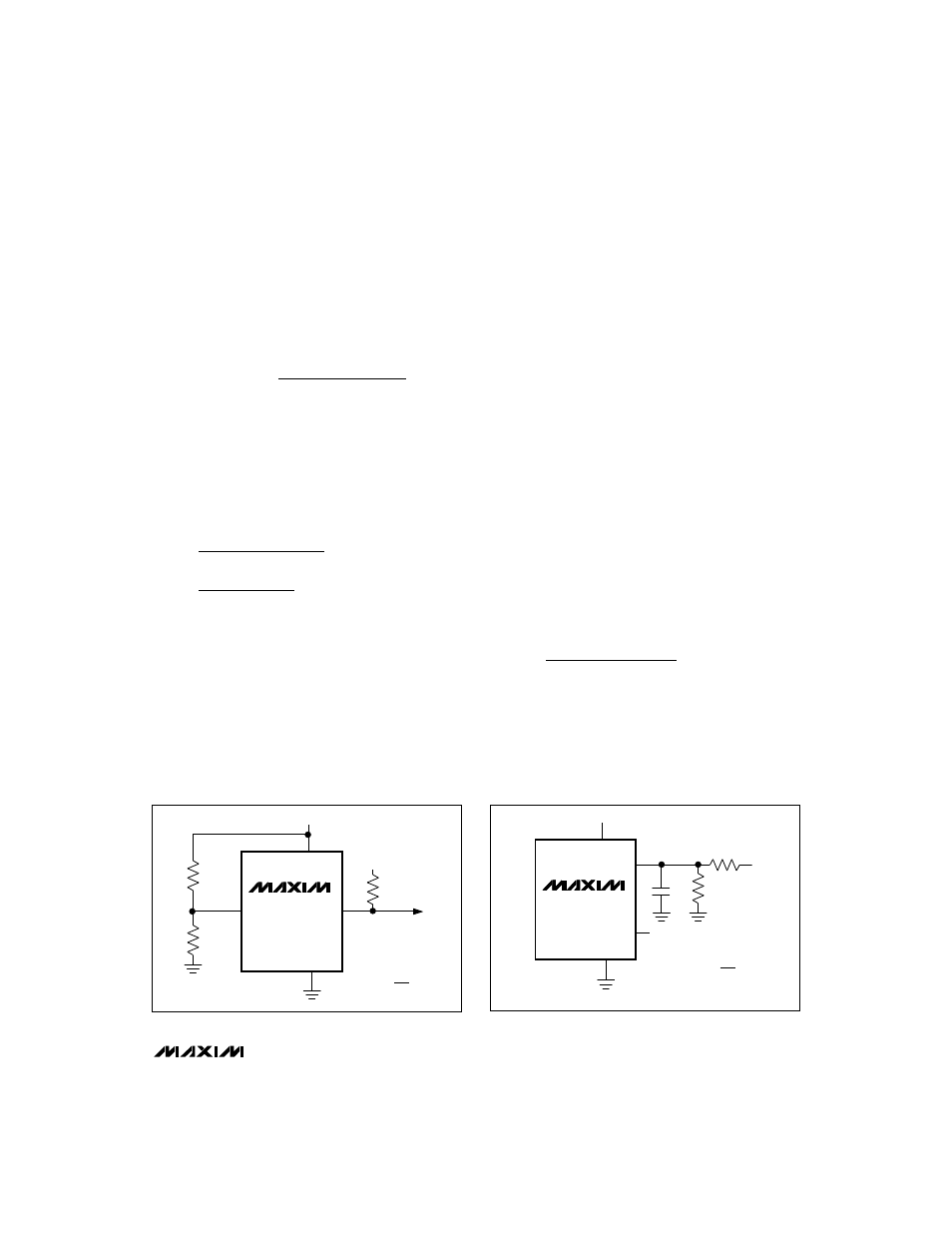
GND
MAX747
V+
FB
12
5
13
V
IN
...to V
OUT
R4 = 10k
Ω
TO 1M
Ω
OUT
8
R5
R4
C6
*
( )
R5 = R4 -1
V
OUT
2V
*
SEE
COMPENSATION CAPACITOR SECTION
N.C.
GND
MAX747
V+
LBO
12
14
13
…
TO V
OUT
OR V
IN
V
TH
= 2.0V
R3
100k
( )
R
2
= R1 -1
V
TRIP
V
TH
1
R2
R1
LOW-BATTERY
OUTPUT
V
IN
LBI
Figure 4. Input Voltage Monitor Circuit
Figure 5. Adjustable Output Circuit