Absolute maximum ratings, Electrical characteristics – Rainbow Electronics MAX747 User Manual
Page 2
MAX747
High-Efficiency PWM, Step-Down
P-Channel DC-DC Controller
2
_______________________________________________________________________________________
ABSOLUTE MAXIMUM RATINGS
Supply Voltage V+, AV+ to GND ..............................-0.3V to 17V
AGND to GND..........................................................-0.3V to 0.3V
All Other Pins................................................-0.3V to (V+ + 0.3V)
Reference Current (I
REF
) ....................................................±2mA
Continuous Power Dissipation (T
A
= +70°C)
Plastic DIP (derate 10.00mW/°C above +70°C) ..........800mW
SO (derate 8.33mW/°C above +70°C) .........................667mW
CERDIP (derate 9.09mW/°C above +70°C) .................727mW
Operating Temperature Ranges:
MAX747C_D .......................................................0°C to +70°C
MAX747E_D.....................................................-40°C to +85°C
MAX747MJD ..................................................-55°C to +125°C
Junction Temperature
MAX747C_D/E_D .........................................................+150°C
MAX747MJD ...............................................................+175°C
Storage Temperature Range .............................-65°C to +160°C
Lead Temperature (soldering, 10sec) .............................+300°C
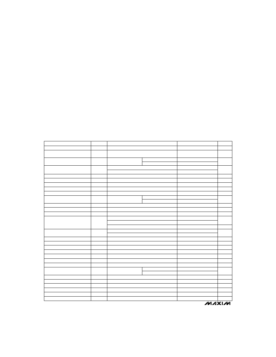
ELECTRICAL CHARACTERISTICS
(V+ = 10V, I
LOAD
= 0mA, I
REF
= 0mA, T
A
= T
MIN
to T
MAX
, unless otherwise noted.)
Stresses beyond those listed under “Absolute Maximum Ratings” may cause permanent damage to the device. These are stress ratings only, and
functional operation of the device at these or any other conditions beyond those indicated in the operational sections of the specifications is not implied.
Exposure to absolute maximum rating conditions for extended periods may affect device reliability.
PARAMETER
SYMBOL
CONDITIONS
MIN
TYP
MAX
UNITS
Input Voltage Range
V+
For regulated outputs
4
15
V
Output Voltage
V
OUT
V+ = 6V to 15V, 0V < V+ - CS < 0.125V, FB = 0V
(includes line and load regulation)
4.85
5.08
5.25
V
Feedback Voltage
1.96
2.00
2.04
V
V+ = 6V to 15V, FB = 0V
0.05
Line Regulation
V+ = 4V to 15V, external feedback mode
0.1
%V
Load Regulation
0V < V+ - CS < 0.125V
1.3
2.5
%
Efficiency
Circuit of Figure 1, I
LOAD
= 0.5A to 2.5A
91
%
OUT Leakage Current
V
OUT
= 5V
50
80
µA
FB Input Logic Low
For dual-mode switchover
40
mV
FB Input Leakage Current
FB = 2V
0.1
100
nA
Reference Voltage
I
REF
= 0µA
1.97
2.00
2.03
V
Reference Load Regulation
I
REF
= 0µA to 100µA
9
20
mV
Soft-Start Source Current
SS = 0V
1
µA
Soft-Start Fault Current
SS = 2V
100
500
µA
Operating, V+ = 15V
0.95
1.3
Operating, V+ = 10V
0.8
mA
Supply Current
Shutdown mode
0.6
20
µA
Oscillator Frequency
f
OSC
MAX747C
85
100
115
kHz
Maximum Duty Cycle
V+ = 6V
91
96
%
CS Amp I
LIM
Threshold
V
LIMIT
V+ - CS
125
150
175
mV
EXT Output High
I
EXT
= -1mA (sourcing)
V+ – 0.1
V
EXT Output Low
I
EXT
= 1mA (sinking)
0.25
V
EXT Sink Current
V
EXT
= 7.5V
110
mA
EXT Source Current
V
EXT
= 2.5V
170
mA
CC Impedance
24
k
Ω
LBI Threshold Voltage
V
TH
LBI falling
1.97
2.00
2.03
V
LBI Input Leakage Current
LBI = 2.5V
100
nA
SHDN Input Voltage Low
V
IL
0.4
V
SHDN Input Voltage High
V
IH
2.0
V
SHDN Input Leakage Current
SHDN = 10V
0.1
100
nA
V
REF
LBO Output Leakage Current
V+ = 15V, LBO = 15V, LBI = 2.5V
1
µA
LBO Output Voltage Low
I
SINK
= 0.5mA
0.4
V
MAX747C
MAX747EM
1.96
2.00
2.04
MAX747E/M
80
100
120
MAX747C
MAX747E/M
1.96
2.00
2.04
V+ - CS = 0V, external
feedback mode
MAX747C
MAX747E/M
1.95
2.00
2.05