Rainbow Electronics MAX747 User Manual
Page 6
MAX747
High-Efficiency PWM, Step-Down
P-Channel DC-DC Controller
6
_______________________________________________________________________________________
Operating Principle
Figure 2 is the MAX747 block diagram. The MAX747
regulates using an inner current-feedback loop and an
outer voltage-feedback loop. The current loop is
stabilized by a slope compensation scheme and the
voltage loop is stabilized by the dominant pole formed
by the filter output capacitor and the load.
Discontinuous-/Continuous-
Conduction Modes
The MAX747 operates in continuous-conduction mode
(CCM) under heavy loads, but operates in
discontinuous-conduction mode (DCM) at light loads,
making it ideal for variable load applications. In DCM,
the inductor current starts and ends at zero on each
cycle. In CCM, the inductor current never returns to zero.
It is composed of a small AC component superimposed
on a DC level, which results in higher load-current
capability and lower output noise. Output noise is
reduced because the inductor does not exhibit the
ringing that occurs when the inductor current reaches
zero, and because there is a smaller AC component in
the inductor-current waveform (see inductor waveforms
in the
Typical Operating Characteristics section). Note
that to transfer equal amounts of energy to the load in
one cycle, the peak current level for the discontinuous
waveform must be much larger than the continuous
waveform peak current.
Slope Compensation
Stability of the inner current-feedback loop is provided
by a slope-compensation scheme that adds a ramp
signal to the current-sense amplifier output. Ideal slope
compensation can be achieved by adding a linear
ramp with the same slope as the
declining
inductor
current to the rising inductor current-sense voltage.
Therefore, the inductor must be scaled to the current-
sense resistor value.
Overcompensation adds a pole to the outer voltage-
feedback loop response that degrades loop stability.
This may cause voltage-mode pulse-frequency-
modulation instead of PWM operation. Under-
compensation results in inner current-feedback loop
instability, and may cause the inductor current to
staircase. Ideal matching between the sense resistor
and inductor is not required. The matching can be
±30% or more.
AV+
GND
MAX747
VIN
(7.5V TO15V)
C2
100µF
V+
C6
470pF
C4
0.1µF
C5
0.22µF
CC
SS
REF
FB
SHDN
AGND
OUT
C1
430
µ
F
5V
@ 2.3A
CS
RSENSE
50m
Ω
P
EXT
L1
50
µ
H
LBO
LBI
R1
R2
R3
100k
6
2
3
5
4
10
14
1
12
7
9
11
8
D1
NSQ03A03
C3
0.1
µ
F
Q1
SI9405DY
13
C7
0.1
µ
F
C1
430
µ
F
AV+
GND
MAX747
VIN
(4.5V TO 15V)
C2
100µF
V+
C4
0.1µF
C5
0.22µF
CC
SS
REF
SHDN
AGND
FB
3.3V
@ 2.3A
CS
RSENSE
50m
Ω
P
EXT
L1
33µH
LBO
LBI
OUT
R1
R2
R3
100k
6
2
3
4
10
14
1
8
12
7
9
11
5
D1
NSQ03A03
C3
0.1
µ
F
Q1
SI9405DY
13
C6
2.7nF
R4
20k
R5
13k
N.C.
N.C.
C1
880
µ
F
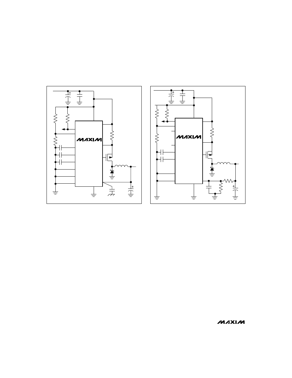
Figure 1b. +3.3V Standard Application Circuit
Figure 1a. +5V Standard Application Circuit