Multirange inputs, serial 14-bit adcs, Analog input circuitry, Analog input bandwidth – Rainbow Electronics MAX1035 User Manual
Page 15: Analog input range and fault tolerance
Analog Input Circuitry
The analog inputs can be individually configured for
either differential or single-ended conversions by writing
the associated analog input configuration byte (Table 2).
The analog input signal source must be capable of dri-
ving the ADC’s 6k
Ω input resistance (Figure 6).
Figure 6 shows the simplified analog input circuit. The
analog inputs are ±6V fault tolerant and are protected
by back-to-back diodes. The summing junction voltage,
V
SJ
, is a function of the channel’s input common-mode
voltage:
As a result, the analog input impedance is relatively
constant over the input voltage as shown in Figure 5.
Single-ended conversions are internally referenced to
AGND1 (Tables 3 and 4). In differential mode, IN+ and
IN- are selected according to Tables 3 and 5. When con-
figuring differential channels, the differential pair follows
the analog configuration byte for the positive channel.
For example, to configure CH2 and CH3 for a ±V
REF
dif-
ferential conversion, set the CH2 analog configuration
byte for a differential conversion with the ±V
REF
range
(1010 1100). To initiate a conversion for the CH2 and
CH3 differential pair, issue the command 1010 0000.
Analog Input Bandwidth
The MAX1034/MAX1035 input-tracking circuitry has a
1.5MHz small-signal bandwidth. The 1.5MHz input
bandwidth makes it possible to digitize high-speed
transient events. Harmonic distortion increases when
digitizing signal frequencies above 15kHz as shown in
the THD, -SFDR vs. Analog Input Frequency plot in the
Typical Operating Characteristics.
Analog Input Range and Fault Tolerance
Figure 7 illustrates the software-selectable single-
ended analog input voltage range that produces a valid
digital output. Each analog input channel can be inde-
pendently programmed to one of seven single-ended
input ranges by setting the R[2:0] control bits with
DIF/SGL = 0.
V
R
R
R
V
R
R
R
V
SJ
CM
.
=
+
Ч
+
+
+
Ч
1
1
2
2 375
1
1
1
2
MAX1034/MAX1035
8-/4-Channel, ±V
REF
Multirange Inputs,
Serial 14-Bit ADCs
______________________________________________________________________________________
15
CS
SCLK
1
2
3
4
5
6
7
8
9
10
11
12
13
14
15
16
17
18
19
20
21
22
23
24
25
26
27
28
29
30
31
32
DIN
S
C2
C1
C0
0
0
0
0
ANALOG INPUT
TRACK AND HOLD*
DOUT
B13
B12
B11
B10
B9
B8
B7
B6
B5
B4
B3
B2
B1
B0
X
X
BYTE 1
BYTE 2
BYTE 3
BYTE 4
SSTRB
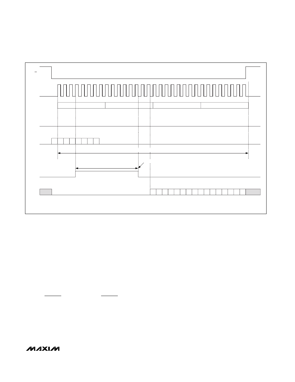
HOLD
TRACK
HOLD
HIGH
IMPEDANCE
t
ACQ
*TRACK AND HOLD TIMING IS CONTROLLED BY SCLK.
f
SAMPLE
≈ f
SCLK
/ 32
SAMPLING INSTANT
HIGH
IMPEDANCE
Figure 2. External Clock-Mode Conversion (Mode 0)