Multirange inputs, serial 14-bit adcs, Detailed description, Pin description (continued) – Rainbow Electronics MAX1035 User Manual
Page 13
Detailed Description
The MAX1034/MAX1035 multirange, low-power, 14-bit
successive-approximation ADCs operate from a single
+5V supply and have a separate digital supply allowing
digital interface with 2.7V to 5.25V systems. These 14-bit
ADCs have internal track-and-hold (T/H) circuitry that
supports single-ended and fully differential inputs. For
single-ended conversions, the valid analog input voltage
range spans from -V
REF
below ground to +V
REF
above
ground. The maximum allowable differential input volt-
age spans from -2 x V
REF
to +2 x V
REF
. Data can be
converted in a variety of software-programmable chan-
nel and data-acquisition configurations. Microprocessor
(µP) control is made easy through an SPI-/QSPI-/
MICROWIRE-compatible serial interface.
MAX1034/MAX1035
8-/4-Channel, ±V
REF
Multirange Inputs,
Serial 14-Bit ADCs
______________________________________________________________________________________
13
Pin Description (continued)
PIN
MAX1034
MAX1035
NAME
FUNCTION
21
18
AGND3
Analog Signal Ground 3. AGND3 is the ADC negative reference potential. Connect AGND3 to
AGND1. DGND, DGNDO, AGND3, AGND2, and AGND1 must be connected together.
22
19
AV
DD2
Analog Supply Voltage 2. Connect AV
DD2
to a +4.75V to +5.25V power-supply voltage.
Bypass AV
DD2
to AGND2 with a 0.1µF capacitor.
23
20
AGND2
Analog Ground 2. This ground carries approximately five times more current than AGND1.
DGND, DGNDO, AGND3, AGND2, and AGND1 must be connected together.
24
1
AGND1
Anal og Gr ound 1. D GN D , D GN DO, AGN D 3, AGN D 2, and AGND 1 must b e connected together .
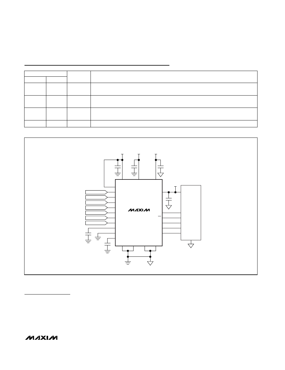
4–20mA
PLC
ACCELERATION
PRESSURE
TEMPERATURE
WHEATESTONE
WHEATESTONE
1
µF
0.1
µF
AGND2
DGNDO
AGND3
DGND
AV
DD2
DV
DD
AV
DD1
0.1
µF
0.1
µF
0.1
µF
5.0V
5.0V
5.0V
MAX1034
CHO
CH1
CH2
CH3
CH4
CH5
CH6
CH7
REF
AGND1
REFCAP
0.1
µF
3.3V
MC68HCXX
µC
DV
DDO
SCLK
CS
DIN
SSTRB
DOUT
V
DD
SCK
I/O
MOSI
I/O
MISO
V
SS
Figure 1. Typical Application Circuit