/4-channel, ±v, Multirange inputs, serial 14-bit adcs, Table 2. analog input configuration byte – Rainbow Electronics MAX1035 User Manual
Page 14
MAX1034/MAX1035
The MAX1034 has eight single-ended analog input
channels or four differential channels (see the Block
Diagram at the end of the data sheet). The MAX1035
has four single-ended analog input channels or two dif-
ferential channels. Each analog input channel is inde-
pendently software programmable for seven
single-ended input ranges (0 to +V
REF
/2,
-V
REF
/2 to 0, 0 to +V
REF
, -V
REF
to 0, ±V
REF
/4, ±V
REF
/2,
and ±V
REF
) and three differential input ranges (±V
REF
/2,
±V
REF
, and ±2 x V
REF
). Additionally, all analog input
channels are fault tolerant to ±6V. A fault condition on
an idle channel does not affect the conversion result of
other channels.
Power Supplies
To maintain a low-noise environment, the MAX1034 and
MAX1035 provide separate power supplies for each
section of circuitry. Table 1 shows the four separate
power supplies. Achieve optimal performance using
separate AV
DD1
, AV
DD2
, DV
DD
, and DV
DDO
supplies.
Alternatively, connect AV
DD1
, AV
DD2
, and DV
DD
together as close to the device as possible for a conve-
nient power connection. Connect AGND1, AGND2,
AGND3, DGND, and DGNDO together as close to the
device as possible. Bypass each supply to the corre-
sponding ground using a 0.1µF capacitor (Table 1). If
significant low-frequency noise is present, add a 10µF
capacitor in parallel with the 0.1µF bypass capacitor.
Converter Operation
The MAX1034/MAX1035 ADCs feature a fully differen-
tial, successive-approximation register (SAR) conver-
sion technique and an on-chip T/H block to convert
voltage signals into a 14-bit digital result. Both single-
ended and differential configurations are supported
with programmable unipolar and bipolar signal ranges.
Track-and-Hold Circuitry
The MAX1034/MAX1035 feature a switched-capacitor
T/H architecture that allows the analog input signal to be
stored as charge on sampling capacitors. See Figures 2,
3, and 4 for T/H timing and the sampling instants for
each operating mode. The MAX1034/MAX1035 analog
input circuitry buffers the input signal from the sampling
capacitors, resulting in a constant analog input current
with varying input voltage (Figure 5).
8-/4-Channel, ±V
REF
Multirange Inputs,
Serial 14-Bit ADCs
14
______________________________________________________________________________________
Table 1. MAX1034/MAX1035 Power Supplies and Bypassing
POWER
SUPPLY/GROUND
SUPPLY VOLTAGE
RANGE (V)
TYPICAL SUPPLY
CURRENT (mA)
CIRCUIT SECTION
BYPASSING
DV
DDO
/DGNDO
2.7 to 5.25
0.2
Digital I/O
0.1µF to DGNDO
AV
DD2
/AGND2
4.75 to 5.25
17.5
Analog Circuitry
0.1µF to AGND2
AV
DD1
/AGND1
4.75 to 5.25
3.0
Analog Circuitry
0.1µF to AGND1
DV
DD
/DGND
4.75 to 5.25
0.9
Digital Control Logic and
Memory
0.1µF to DGND
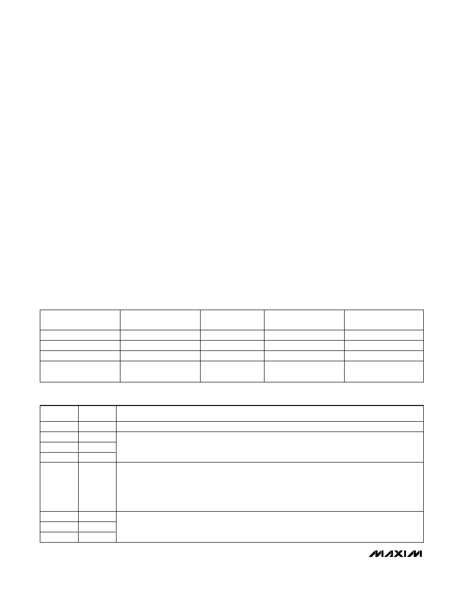
Table 2. Analog Input Configuration Byte
BIT
NUMBER
NAME
DESCRIPTION
7
START
Start Bit. The first logic 1 after
CS goes low defines the beginning of the analog input configuration byte.
6
C2
5
C1
4
C0
Channel-Select Bits. SEL[2:0] select the analog input channel to be configured (Tables 4 and 5).
3
DIF/
SGL
Differential or Single-Ended Configuration Bit. DIF/
SGL = 0 configures the selected analog input channel
for single-ended operation. DIF/
SGL = 1 configures the channel for differential operation. In single-ended
mode, input voltages are measured between the selected input channel and AGND1, as shown in
Table 4. In differential mode, the input voltages are measured between two input channels, as shown in
Table 5. Be aware that changing DIF/
SGL adjusts the FSR, as shown in Table 6.
2
R2
1
R1
0
R0
Input-Range-Select Bits. R[2:0] select the input voltage range, as shown in Table 6 and Figure 7.