Rainbow Electronics MAX768 User Manual
Page 9
MAX768
Low-Noise, Dual-Output, Regulated Charge Pump
for GaAsFET, LCD, and VCO Supplies
_______________________________________________________________________________________
9
Switching-Frequency Control
For applications sensitive to the MAX768’s internal
switching frequency, connect an external TTL/CMOS
(within IN and GND) clock to SYNC. The clock must be
a 20kHz to 240kHz square wave between 40% and
60% duty cycle.
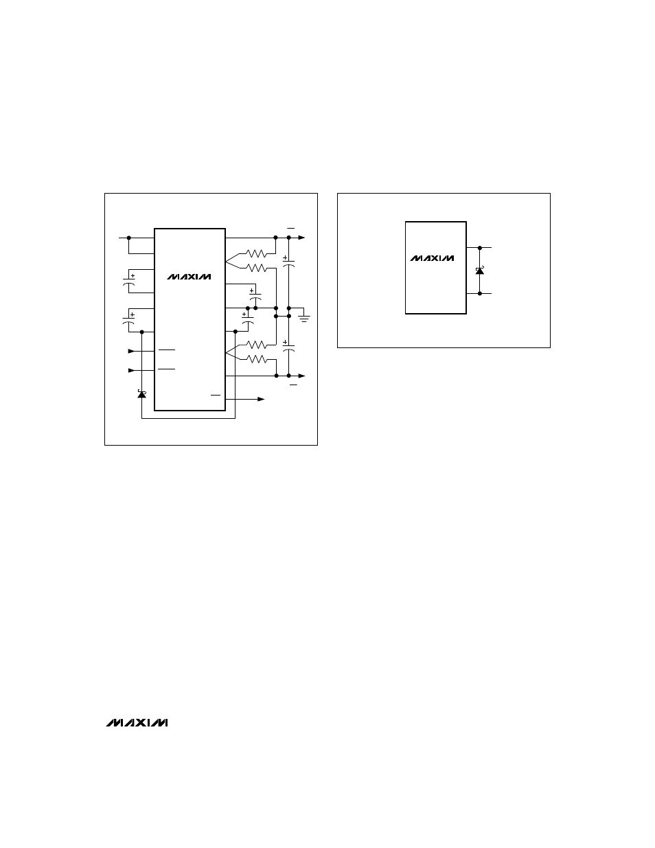
Schottky Diodes
When under heavy loads, where POUT is sourcing into
NOUT (i.e., load current flows from POUT to NOUT,
rather than from supply to ground), do not allow NOUT
to pull above ground. In applications where large cur-
rents from POUT to NOUT are likely, use a Schottky
diode (1N5817) between GND and NOUT, with the
anode connected to GND (Figure 4).
Connect a IN5817-type Schottky diode from C2- to V-
to assure proper start-up.
Layout and Grounding
Good layout is important, primarily for good noise per-
formance:
1) Mount all components as close together as possi-
ble.
2) Keep traces short to minimize parasitic inductance
and capacitance. This includes connections to
SETP and SETN.
3) Use a ground plane.
Noise and Ripple Measurement
Accurately measuring output noise and ripple can be
difficult. Brief differences in ground potential between
the circuit and the oscilloscope (which result from the
charge pump’s switching action) cause ground cur-
rents in the probe’s wires, inducing sharp voltage
spikes. For best results, measure directly across output
capacitor C3, C4, C5, or C6. Do not use the oscillo-
scope probe’s ground lead; instead, remove the
cover’s ground lead and touch the ground ring on the
probe directly to the ground terminal of C3, C4, C5, or
C6. Or, use a Tektronix chassis-mount test jack (part
no. 131-0258) to connect your scope probe directly.
This direct connection provides the most accurate
noise and ripple measurement.
MAX768
IN
SYNC
C2
C1
V
IN
C1+
C1-
C2+
C3
C5
C6
R2
R1
R3
R4
R4
R3
C4
V
NOUT
= (-1.25) (1 + )
C2-
NSHDN
PSHDN
POUT
SETP
V+
GND
V-
SETN
NOUT
RDY
R2
R1
V
POUT
= (1.25) (1+ )
Figure 3. MAX768 Adjustable Configuration
MAX768
GND
NOUT
Figure 4. A Schottky diode protects the MAX768 when a large
current flows from POUT to NOUT.