Detailed description, Applications information – Rainbow Electronics MAX768 User Manual
Page 7
MAX768
Low-Noise, Dual-Output, Regulated Charge Pump
for GaAsFET, LCD, and VCO Supplies
_______________________________________________________________________________________
7
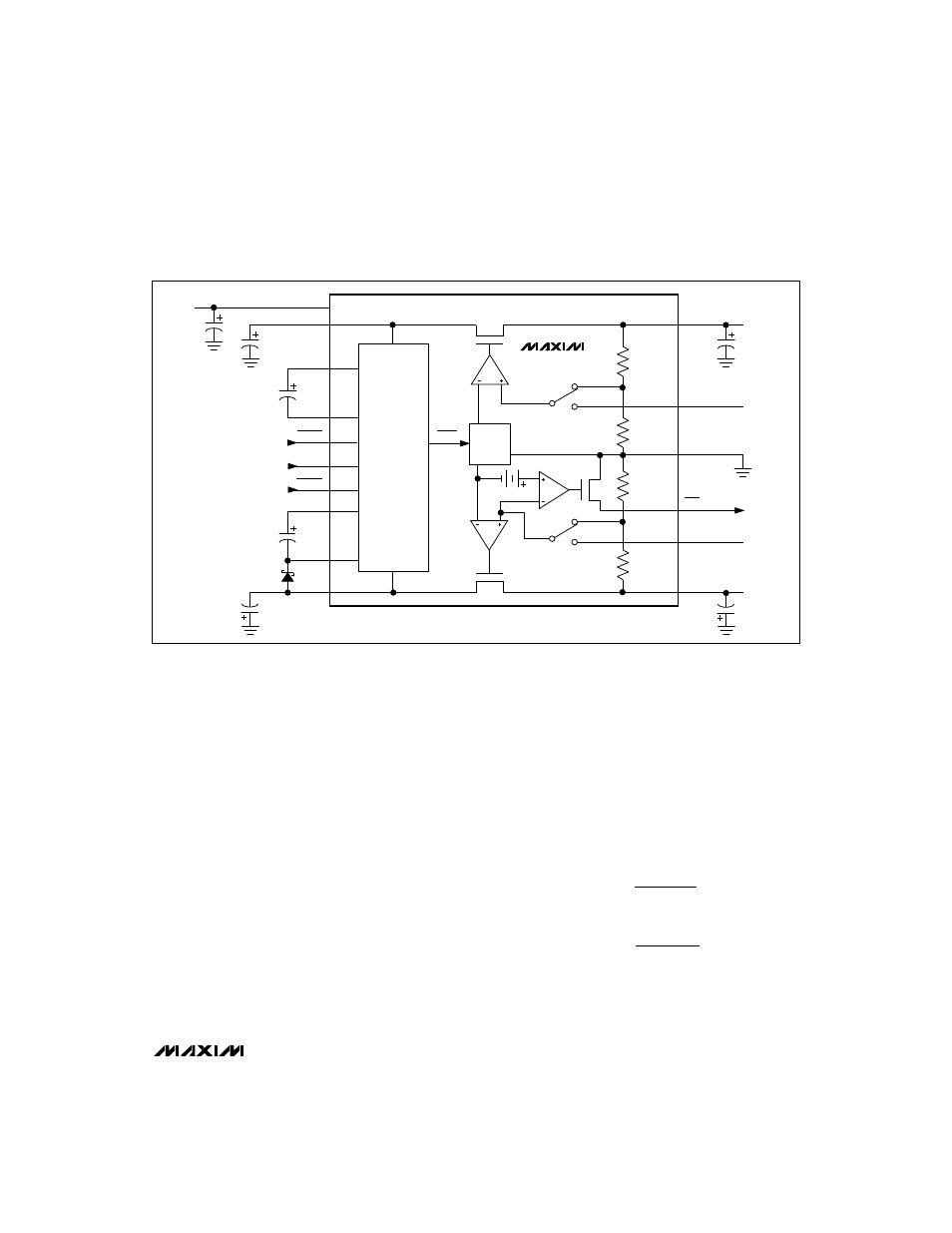
_______________Detailed Description
The MAX768 requires only seven external capacitors to
implement a regulated voltage doubler/inverter. These
can be ceramic or polarized electrolytic capacitors rang-
ing from 2.2µF to 47µF. Figure 1 is a functional diagram of
the MAX768. The applied input voltage (V
IN
) is first dou-
bled to a value of 2V
IN
by a capacitor charge pump and
then stored in the V+ reservoir capacitor. Next, the volt-
age at V+ is inverted to -2V
IN
and stored at the V- reser-
voir capacitor. The voltages at V+ and V- are then linear
regulated and appear at POUT and NOUT, respectively.
The ripple noise induced by the doubling and inverting
charge pump is reduced by the linear regulators to
1.2mVp-p for POUT and 1.7mVp-p for NOUT. In addition,
the linear regulator’s excellent AC rejection attenuates
noise from the incoming supply. A minimum of 5mA is
available at each output. When NOUT is more negative
than 90% of the regulated output voltage, the open-drain
RDY output pulls to GND.
The charge pump operates in three modes: when
SYNC
= GND, the charge pump operates at 25kHz; when
SYNC = IN, it operates at 100kHz, or SYNC can be over-
driven with an external clock in the 20kHz to 240kHz
range. The clock must have a 40% to 60% duty cycle.
__________Applications Information
Setting the Output Voltage
Connect SETP or SETN directly to GND to select a fixed
+5V or -5V output voltage, respectively (Figure 2).
Select an alternative voltage for either output by con-
necting SETP or SETN to the midpoint of a resistor volt-
age divider from POUT or NOUT, respectively, to GND
(Figure 3). (2 x V
IN
) must be 1.0V above the absolute
value of the output voltage to ensure proper regulation.
Calculate the output voltage from the formulas below.
Choose R1 and R3 at between 100k
Ω
to 400k
Ω
.
where V
PSET REF
= 1.25V (typical) and
V
NSET REF
= -1.25V (typical).
R2 = R1
R4 = R3
( )
−
( )
−
V
V
V
V
POUT
PSET REF
NOUT
NSET REF
1
1
MAX768
VOLTAGE
DOUBLER
+1.25V
REF
-1.25V
SHDN
POUT
SETP
CONNECT TO GND
TO SET V
POUT
= +5V
CONNECT TO GND
TO SET V
NOUT
= -5V
GND
RDY
SETN
NOUT
IN
V+
C1+
C1-
PSHDN
SYNC
NSHDN
C2+
C2-
N
N
P
V-
VOLTAGE
INVERTER
Figure 1. Functional Diagram