Max2036, Ultrasound vga integrated with cw octal mixer, Table 1. summary of cwd beamforming methods – Rainbow Electronics MAX2036 User Manual
Page 16
MAX2036
CW Mixer Output Summation
The outputs from the octal mixer array are summed inter-
nally to produce the total CWD summed beamformed
signal. The octal array produces eight differential quad-
rature (Q) outputs and eight differential in-phase (I) out-
puts. All quadrature and in-phase outputs are summed
into single I and Q differential current outputs
(CW_QOUT+, CW_QOUT-, CW_IOUT+, CW_IOUT-).
LO Phase Select
The LO phase dividers can be programmed through
the shift registers to allow for 4, 8, or 16 quadrature
phases for a complete CW beamforming solution.
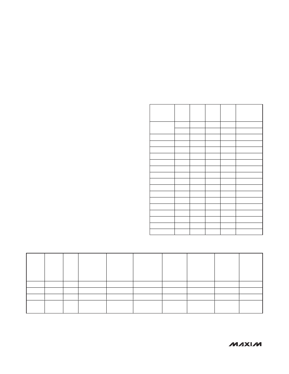
CWD Beamforming Modes
There are four separate modes of operating the CWD
beamformer. See Table 1 for a summary of the different
modes of operation. The mode of operation can be
selected by the CW_M1 and CW_M2 logic inputs.
Phase generation is controlled through the serial inter-
face. See the
Serial Interface
section in the
Applications
Information
section for details on how to program for
different quadrature phases.
Mode 1
For mode 1 operation, the LO_LVDS input frequency is
typically 16 x f
LO
. As the CWD LO frequency range is
1MHz to 7.5MHz, the input frequency ranges from
16MHz to 120MHz. This high LO clock frequency
requires a differential LVDS input. The 16 x f
LO
input is
then divided by 16 to produce 16 phases. These 16
phases are generated for each of the 8 channels and
programmed for the selected phase by a serial shift
register. Each channel has a corresponding 5-bit shift
register, which is used to program the output phase of
the divide-by-16 circuit. The first 4 bits of the shift regis-
ter are for programming the 16 phases; the fifth bit turns
each channel on/off individually. For mode 1, set both
CW_M1 and CW_M2 to a logic-low. See Table 2.
Ultrasound VGA Integrated
with CW Octal Mixer
16
______________________________________________________________________________________
CW_M1
CW_M2
MODE
LO INPUT
FREQUENCY
CLOCK
INTERFACE
PHASE
R ESO L U T IO N
NO. OF
CLOCK
INPUTS
PER CHIP
PROGRAM
BY SERIAL
SHIFT
REGISTER
(SSR)
NO. OF
USEFUL
BITS IN
SSR
NO. OF
DON’T-
CARE
BITS IN
SSR
0
0
1
16 x
LVDS
16 phases
1
Yes
4
0
0
1
2
8 x
LVDS
8 phases
1
Yes
3
1 MSB
1
0
3
4 x
3V CMOS
4 phases
8
Yes
2
2 MSBs
1
1
4
4 x
3V CMOS
Quadrature
provided
8
No
N/A
N/A
Table 1. Summary of CWD Beamforming Methods
MODE 1
CW_M1 = 0
CW_M2 = 0
MSB
LSB
SHUTDOWN
D
C
B
A
SD
PHASE
(DEG)
(B0)
(B1)
(B2)
(B3)
(B4)
0
0 0 0 0
0/1
22.5 0 0 0 1
0/1
45
0 0 1 0
0/1
67.5 0 0 1 1
0/1
90
0 1 0 0
0/1
112.5 0 1 0 1
0/1
135 0 1 1 0
0/1
157.5 0 1 1 1
0/1
180 1 0 0 0
0/1
202.5 1 0 0 1
0/1
225 1 0 1 0
0/1
247.5 1 0 1 1
0/1
270 1 1 0 0
0/1
292.5 1 1 0 1
0/1
315 1 1 1 0
0/1
337.5 1 1 1 1
0/1
Table 2. Mode 1 Logic Table (B4 = 0:
Channel On/B4 = 1 Channel Off)
N/A = Not applicable.