Table 1. typical available output current, Table 2. selecting the operating mode, Step-up converter – Rainbow Electronics MAX1703 User Manual
Page 9
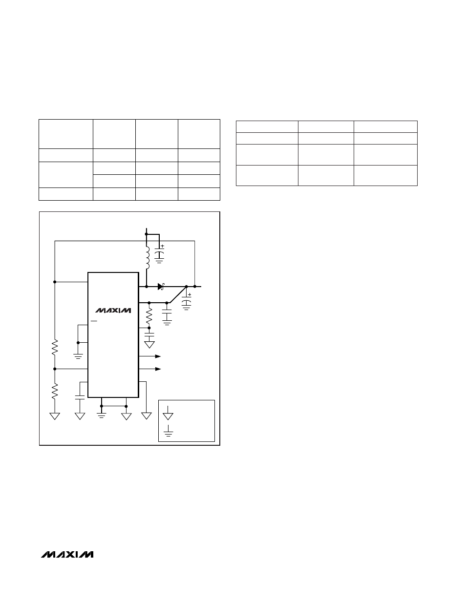
Table 1. Typical Available Output Current
Additional features include synchronous rectification for
high efficiency and improved battery life, and an
uncommitted comparator (POK) for monitoring the reg-
ulator’s output or battery voltage. The MAX1703 also
includes a gain block that can be used to build a linear
regulator using an external P-channel MOSFET pass
device; this gain block can also function as a second
comparator. A CLK input allows frequency synchro-
nization to reduce interference.
Table 2. Selecting the Operating Mode
Step-Up Converter
The step-up switching DC-DC converter generates an
adjustable output from 2.5V to 5.5V. The internal N-
channel MOSFET switch is turned on during the first
part of each cycle, allowing current to ramp up in the
inductor and store energy in a magnetic field. During
the second part of each cycle, when the MOSFET is
turned off, the voltage across the inductor reverses and
forces current through the diode and synchronous rec-
tifier to the output filter capacitor and load. As the ener-
gy stored in the inductor is depleted, the current ramps
down and the output diode and synchronous rectifier
turn off. Depending on the CLK/SEL pin setting, voltage
across the load is regulated using either low-noise
PWM or low-power operation (Table 2).
Low-Noise PWM Operation
When CLK/SEL is pulled high, the MAX1703 operates
in a high-power, low-noise PWM mode. During PWM
operation, the MAX1703 switches at a constant fre-
quency (300kHz), and modulates the MOSFET-switch
pulse width to control the power transferred per cycle
and regulate the voltage across the load. In PWM mode
the device can output up to 1.5A. Switching harmonics
generated by fixed-frequency operation are consistent
and easily filtered. See the Noise Spectrum plot in the
Typical Operating Characteristics
.
During PWM operation, each of the internal clock’s ris-
ing edges sets a flip-flop, which turns on the N-channel
MOSFET switch (Figure 3). The switch turns off when
the sum of the voltage-error, slope-compensation, and
current-feedback signals trips a multi-input comparator
and resets the flip-flop; the switch remains off for the
rest of the cycle. When a change occurs in the output
voltage error signal, the comparator shifts the level to
which the inductor current ramps during each cycle. A
second comparator enforces an inductor current limit of
2.7A (typical).
MAX1703
1-Cell to 3-Cell, High-Power (1.5A),
Low-Noise, Step-Up DC-DC Converter
_______________________________________________________________________________________
9
2.4
2 NiCd/NiMH
2.4
3.6
3 NiCd/NiMH
NO. OF CELLS
1.2
1 NiCd/NiMH
INPUT
VOLTAGE
(V)
5.0
3.3
5.0
3.3
OUTPUT
VOLTAGE
(V)
950
1400
1600
600
OUTPUT
CURRENT
(mA)
GND
PGND
AO
POUT
OUT
LXP, LXN
D1
C1
100
µ
F
MBR0520L
V
BATT
C4
2 x 220
µ
F
L1
4.7
µ
H
POK
FB
REF
CLK/SEL
ON
AIN
POKIN
C3
0.22
µ
F
R3
R4
C2
0.22
µ
F
NOTE: HEAVY LINES INDICATE HIGH-CURRENT PATHS.
C5
0.22
µ
F
R5
10
Ω
MAX1703
SIGNAL GROUND
POWER GROUND
Figure 2. MAX1703 in High-Power PWM Mode
Synchronized
PWM
External Clock
(200kHz to 400kHz)
PWM
1
Low power
MODE
0
CLK/SEL
Low noise,
high output current
Low noise,
high output current
Low supply current
FEATURES