Shutdown, Power-good (pok) comparator, Reference – Rainbow Electronics MAX1703 User Manual
Page 11: Gain block
Shutdown
The MAX1703 shuts down to reduce quiescent current
to 1µA. During shutdown (ON = V
OUT
), the reference,
low-battery comparator, gain block, and all feedback
and control circuitry are off. The boost converter’s out-
put drops to one Schottky diode drop below the input.
Power-Good (POK) Comparator
The MAX1703 features an uncommitted POK compara-
tor. The internal POK comparator has an open-drain
output (POK) capable of sinking 1mA. When the input
(POKIN) rises above the 1.25V reference, the POK
open-drain output turns off. The POKIN input has 10mV
of hysteresis.
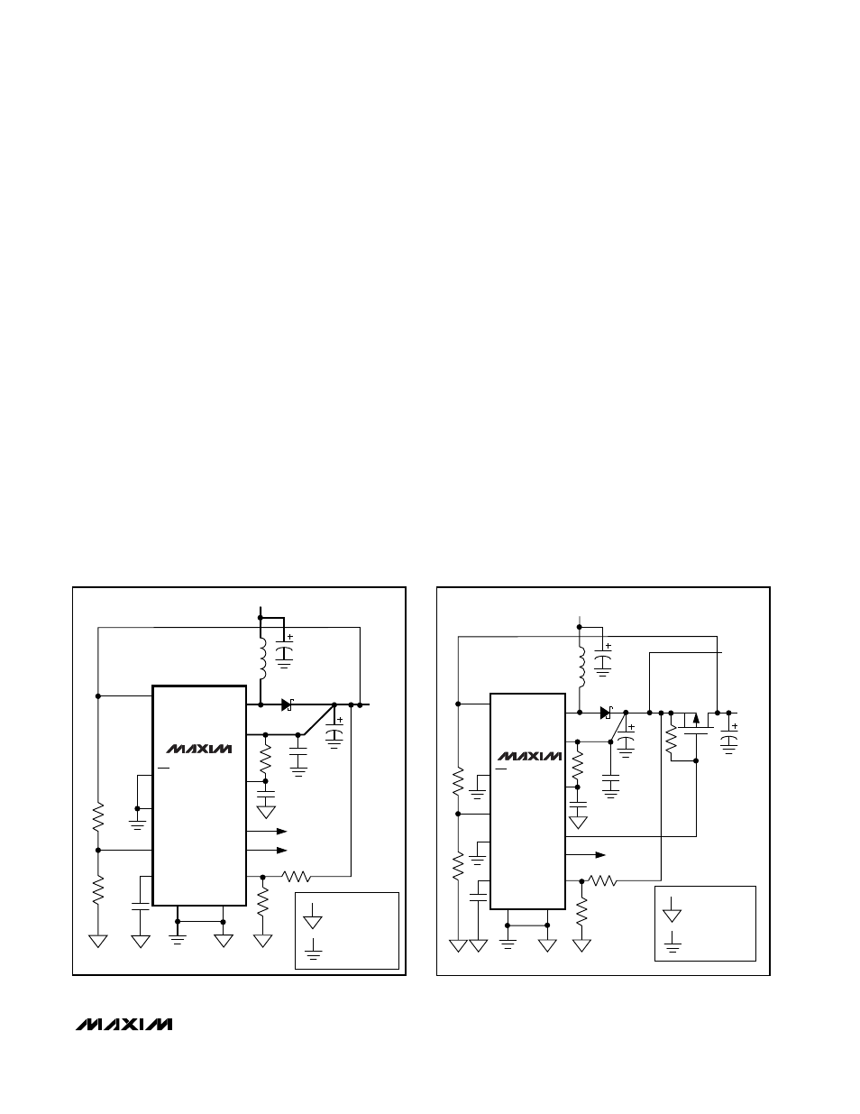
To provide a power-good signal, connect the POKIN
input to an external resistor-divider between OUT and
GND (Figure 5). Calculate the resistor values as follows:
R3 = R4(V
TH
/ V
REF
- 1)
where V
TH
is the desired input voltage trip threshold.
Since the input bias current into POKIN is less than
20nA, R4 can be a large value (such as 270k
Ω
or less)
without sacrificing accuracy. Connect the resistor volt-
age-divider as close to the IC as possible, within 0.2in.
(5mm) of POKIN.
Reference
The MAX1703 has an internal 1.250V, 1% bandgap ref-
erence. Connect a 0.22µF bypass capacitor to GND
within 0.2in. (5mm) of the REF pin. REF can source up
to 50µA of external load current.
Gain Block
The MAX1703 gain block can function as a second
comparator, or can be used to build a linear regulator
using an external P-channel MOSFET pass device. The
gain-block output is a single-stage transconductance
amplifier that drives an open-drain N-channel MOSFET.
The g
m
of the entire gain-block stage is 10mmho.
Figure 6 shows the gain block used in a linear-regulator
application. The output of an external P-channel pass
element is compared to the internal reference. The dif-
ference is amplified and used to drive the gate of the
pass element. Use a logic-level PFET, such as an
NDS336P (R
DS(ON)
= 270m
Ω
) from Fairchild. This con-
figuration allows ripple reduction at the output. If a
lower R
DS(ON)
PFET is used, then the linear regulator
output filter capacitance may need to be increased.
To use the gain block as a comparator, refer to the
Power-Good (POK) Comparator
section.
MAX1703
1-Cell to 3-Cell, High-Power (1.5A),
Low-Noise, Step-Up DC-DC Converter
______________________________________________________________________________________
11
GND
PGND
AO
POUT
OUT
LXP, LXN
D1
MBR0520L
OUTPUT
C1
100
µ
F
V
IN
C4
2 x 220
µ
F
L1
4.7
µ
H
POK
FB
REF
CLK/SEL
ON
AIN
POKIN
C3
0.22
µ
F
R3
R4
C2
0.22
µ
F
NOTE: HEAVY LINES INDICATE HIGH-CURRENT PATHS.
C5
0.22
µ
F
R5
10
Ω
R2
R1
MAX1703
SIGNAL GROUND
POWER GROUND
Figure 5. Adjustable Output (PWM Mode)
GND
PGND
AO
POUT
OUT
LXP, LXN
C1
100
µ
F
MBR0520L
BOOST
OUTPUT
47
µ
F
LINEAR
REGULATED
OUTPUT
R6
20k
C5
0.22
µ
F
C4
330
µ
F
R5
10
Ω
C2
0.22
µ
F
V
IN
L1
4.7
µ
H
POK
FB
REF
CLK/SEL
ON
AIN
POKIN
R3
R4
R2
100k
R1
MAX1703
P
SIGNAL GROUND
POWER GROUND
Figure 6. Using the Gain Block as a Linear Regulator