Rainbow Electronics MAX1213 User Manual
Page 2
MAX1213
1.8V, 12-Bit, 170Msps ADC for
Broadband Applications
2
_______________________________________________________________________________________
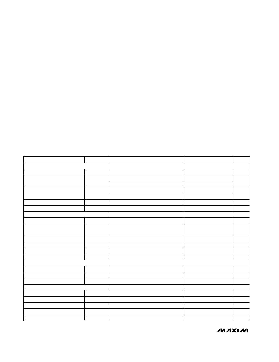
ABSOLUTE MAXIMUM RATINGS
ELECTRICAL CHARACTERISTICS
(AV
CC
= OV
CC
= 1.8V, AGND = OGND = 0, f
SAMPLE
= 170MHz, differential sine-wave clock input drive, 0.1µF capacitor on REFIO,
internal reference, digital output pins differential R
L
= 100Ω ±1%, T
A
= T
MIN
to T
MAX
, unless otherwise noted. ≥+25°C guaranteed by
production test, <+25°C guaranteed by design and characterization. Typical values are at T
A
= +25°C.)
Stresses beyond those listed under “Absolute Maximum Ratings” may cause permanent damage to the device. These are stress ratings only, and functional
operation of the device at these or any other conditions beyond those indicated in the operational sections of the specifications is not implied. Exposure to
absolute maximum rating conditions for extended periods may affect device reliability.
AV
CC
to AGND ..................................................... -0.3V to +2.1V
OV
CC
to OGND .................................................... -0.3V to +2.1V
AV
CC
to OV
CC
...................................................... -0.3V to +2.1V
AGND to OGND ................................................... -0.3V to +0.3V
Analog Inputs to AGND ...........................-0.3V to (AV
CC
+ 0.3V)
All Digital Inputs to AGND........................-0.3V to (AV
CC
+ 0.3V)
REFIO, REFADJ to AGND ........................-0.3V to (AV
CC
+ 0.3V)
All Digital Outputs to OGND ....................-0.3V to (OV
CC
+ 0.3V)
ESD on All Pins (Human Body Model) .............................±2000V
Continuous Power Dissipation (T
A
= +70°C)
68-Pin QFN (derate 41.7mW/°C above +70°C) .........3333mW
Operating Temperature Range ...........................-40°C to +85°C
Junction Temperature .....................................................+150°C
Storage Temperature Range ............................-60°C to +150°C
Maximum Current into Any Pin............................................50mA
Lead Temperature (soldering,10s) ..................................+300°C
PARAMETER
SYMBOL
CONDITIONS
MIN
TYP
MAX
UNITS
DC ACCURACY
Resolution
12
Bits
f
IN
= 10MHz, T
A
= +25
°
C
-1.5
±
0.5
+1.5
Integral Nonlinearity
(Note 1)
INL
f
IN
= 10MHz (Note 2)
-2.35
±
0.5
+2.35
LSB
T
A
= +25
°
C
-1
±
0.25
+1
Differential Nonlinearity (Note 1)
DNL
No missing codes (Note 2)
-1
±
0.25
+1.5
LSB
Transfer Curve Offset
V
OS
T
A
= +25
°
C (Note 1)
-2.5
+2.5
mV
Offset Temperature Drift
40
mV/
°
C
ANALOG INPUTS (INP, INN)
Full-Scale Input Voltage Range
V
FS
T
A
= +25
°
C (Note 1)
1375
1485
1585
mV
P-P
Full-Scale Range Temperature
Drift
130
ppm/
°
C
Common-Mode Input Range
V
CM
1.365 ±0.15
V
Input Capacitance
C
IN
3
pF
Differential Input Resistance
R
IN
3.00
4.3
6.25
k
Ω
Full-Power Analog Bandwidth
FPBW
900
MHz
REFERENCE (REFIO, REFADJ)
Reference Output Voltage
V
REFIO
T
A
= +25
°
C
1.18
1.24
1.30
V
Reference Temperature Drift
90
ppm/
°
C
REFADJ Input High Voltage
V
REFADJ
Used to disable the internal reference
AV
CC
- 0.3
V
SAMPLING CHARACTERISTICS
Maximum Sampling Rate
f
SAMPLE
170
Msps
Minimum Sampling Rate
f
SAMPLE
20
Msps
Clock Duty Cycle
Set by clock-management circuit
40–60
%
Aperture Delay
t
AD
620
ps
Aperture Jitter
t
AJ
0.2
ps
RMS