Max1748 triple-output tft lcd dc-dc converter, Typical operating characteristics (continued), Pin description – Rainbow Electronics MAX1748 User Manual
Page 7
MAX1748
Triple-Output TFT LCD DC-DC Converter
_______________________________________________________________________________________
7
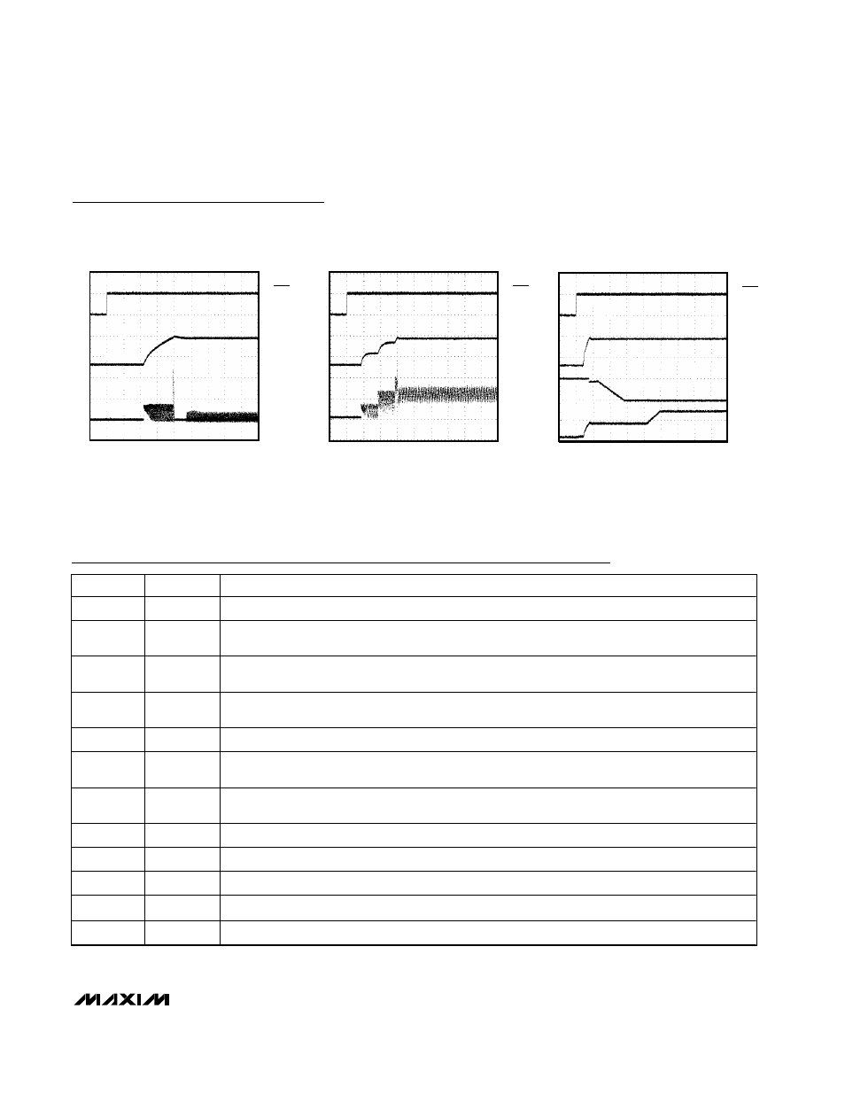
Typical Operating Characteristics (continued)
(Circuit of Figure 5, V
IN
= 3.3V, T
A
= +25°C, unless otherwise noted.)
Pin Description
V
MAIN
5V/div
2V
10V
0
I
LX
500mA/div
MAIN BOOST STARTUP WAVEFORM
MAX1748toc16
1ms/div
R
MAIN
= 1k
Ω, V
MAIN
= 10V
V
SHDN
2V/div
0
0
V
MAIN
5V/div
2V
10V
0
I
LX
500mA/div
MAIN BOOST STARTUP
WAVEFORM WITH LOAD
MAX1748toc17
1ms/div
V
MAIN
= 10V, R
MAIN
= 50
Ω (200mA)
V
SHDN
2V/div
0
0
V
MAIN
5V/div
V
NEG
5V/div
V
POS
10V/div
POWER-UP SEQUENCING
MAX1748toc18
2ms/div
V
MAIN
= 10V, V
NEG
= -5V, V
POS
= 15V
V
SHDN
2V/div
PIN
NAME
FUNCTION
1
RDY
Active-Low Open-Drain Output. Indicates all outputs are ready. The on-resistance is 125
Ω (typ).
2
FB
Main Boost Regulator Feedback Input. Regulates to 1.248V nominal. Connect feedback resistive
divider to analog ground (GND).
3
INTG
Main Boost Integrator Output. If used, connect 470pF to analog ground (GND). To disable
integrator, connect to REF.
4
IN
Supply Input. +2.7V to +5.5V input range. Bypass with a 0.1
µF capacitor between IN and GND, as
close to the pins as possible.
5
GND
Analog Ground. Connect to power ground (PGND) underneath the IC.
6
REF
Internal Reference Bypass Terminal. Connect a 0.22
µF capacitor from this terminal to analog
ground (GND). External load capability to 50
µA.
7
FBP
Positive Charge-Pump Regulator Feedback Input. Regulates to 1.25V nominal. Connect feedback
resistive divider to analog ground (GND).
8
FBN
Negative Charge-Pump Regulator Feedback Input. Regulates to 0V nominal.
9
SHDN
Active-Low Logic-Level Shutdown Input. Connect SHDN to IN for normal operation.
10
DRVN
Negative Charge-Pump Driver Output. Output high level is V
SUPN
, and low level is PGND.
11
SUPN
Negative Charge-Pump Driver Supply Voltage. Bypass to PGND with a 0.1
µF capacitor.
12
DRVP
Positive Charge-Pump Driver Output. Output high level is V
SUPP
, and low level is PGND.