Max1748 triple-output tft lcd dc-dc converter – Rainbow Electronics MAX1748 User Manual
Page 2
MAX1748
Triple-Output TFT LCD DC-DC Converter
2
_______________________________________________________________________________________
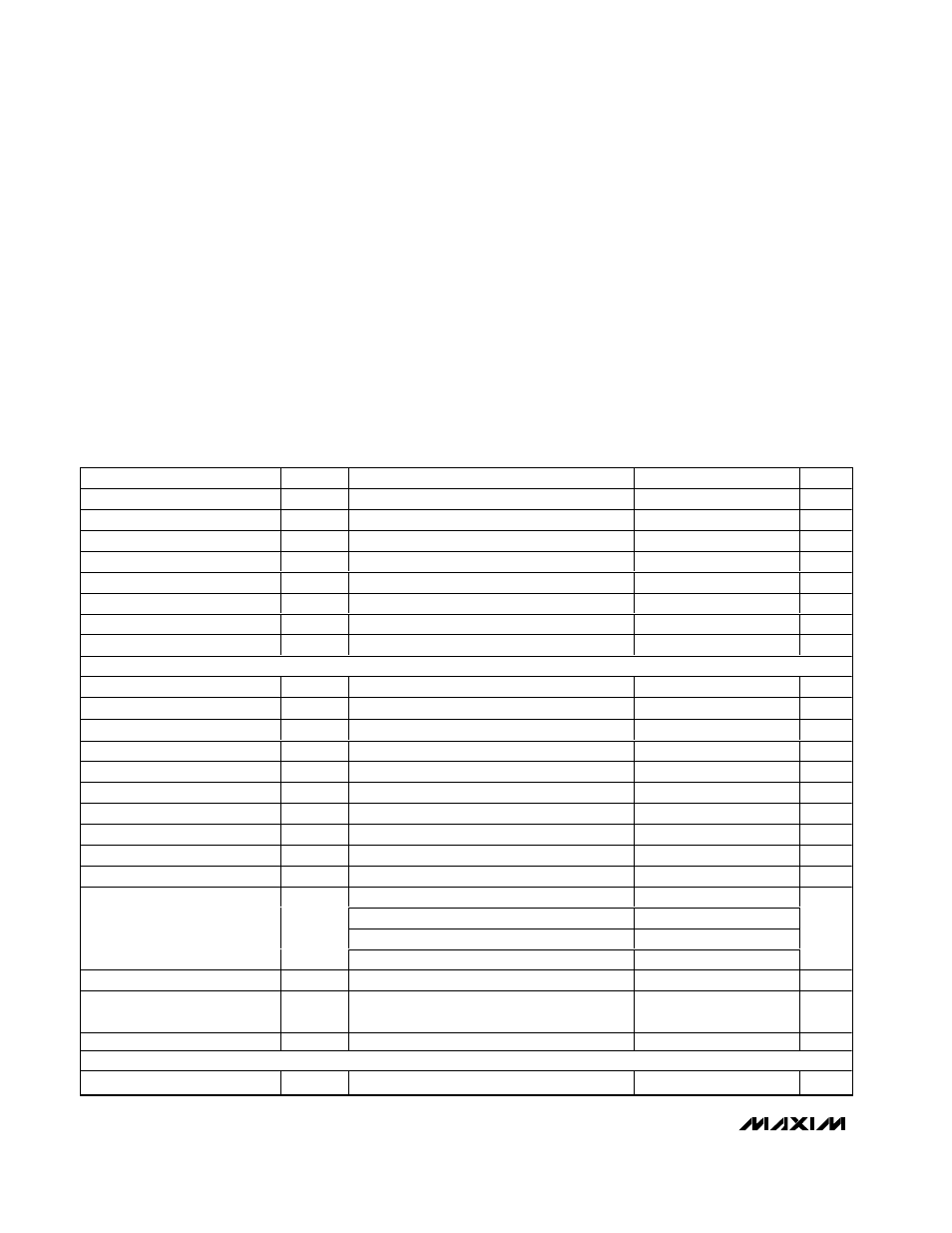
ABSOLUTE MAXIMUM RATINGS
ELECTRICAL CHARACTERISTICS
(V
IN
= +3.0V, SHDN = IN, V
SUPP
= V
SUPN
= 10V, TGND = PGND = GND, C
REF
= 0.22µF, C
INTG
= 470pF, T
A
= 0°C to +85°C, unless
otherwise noted. Typical values are at T
A
= +25°C.)
Stresses beyond those listed under “Absolute Maximum Ratings” may cause permanent damage to the device. These are stress ratings only, and functional
operation of the device at these or any other conditions beyond those indicated in the operational sections of the specifications is not implied. Exposure to
absolute maximum rating conditions for extended periods may affect device reliability.
IN, SHDN, TGND to GND .........................................-0.3V to +6V
DRVN to GND .........................................-0.3V to (V
SUPN
+ 0.3V)
DRVP to GND..........................................-0.3V to (V
SUPP
+ 0.3V)
PGND to GND.....................................................................±0.3V
RDY to GND ...........................................................-0.3V to +14V
LX, SUPP, SUPN to PGND .....................................-0.3V to +14V
INTG, REF, FB, FBN, FBP to GND ...............-0.3V to (V
IN
+ 0.3V)
Continuous Power Dissipation (T
A
= +70°C)
16-Pin TSSOP (derate 9.4mW/°C above +70°C) ..........755mW
Operating Temperature Range
MAX1748EUE .................................................-40°C to +85°C
Junction Temperature ......................................................+150°C
Storage Temperature Range .............................-65°C to +150°C
Lead Temperature (soldering, 10s) .................................+300°C
PARAMETER
SYMBOL
CONDITIONS
MIN
TYP
MAX
UNITS
Input Supply Range
V
IN
2.7
5.5
V
Input Undervoltage Threshold
V
UVLO
V
IN
rising, 40mV hysteresis (typ)
2.2
2.4
2.6
V
IN Quiescent Supply Current
I
IN
V
FB
= V
FBP
= 1.5V, V
FBN
= -0.2V
0.6
1
mA
SUPP Quiescent Current
I
SUPP
V
FBP
= 1.5V
0.4
0.8
mA
SUPN Quiescent Current
I
SUPN
V
FBN
= -0.1V
0.4
0.8
mA
IN Shutdown Current
V
SHDN
= 0, V
IN
= 5V
0.1
10
µA
SUPP Shutdown Current
V
SHDN
= 0, V
SUPP
= 13V
0.1
10
µA
SUPN Shutdown Current
V
SHDN
= 0, V
SUPN
= 13V
0.1
10
µA
MAIN BOOST CONVERTER
Output Voltage Range
V
MAIN
V
IN
13
V
FB Regulation Voltage
V
FB
T
A
= 0
°C to +85°C
1.235
1.248
1.261
V
FB Input Bias Current
I
FB
V
FB
= 1.25V, INTG = GND
-50
50
nA
Operating Frequency
f
OSC
0.85
1
1.15
MHz
Oscillator Maximum Duty Cycle
78
85
90
%
Load Regulation
I
MAIN
= 0 to 200mA, V
MAIN
= 10V
0.2
%
Line Regulation
0.1
% / V
Integrator Gm
320
µmho
LX Switch On-Resistance
R
LX(ON)
I
LX
= 100mA
0.35
0.7
Ω
LX Leakage Current
I
LX
V
LX
= 13V
0.01
20
µA
Phase I = soft-start (1.0ms)
0.275
0.380
0.500
Phase II = soft-start (1.0ms)
0.75
Phase III = soft-start (1.0ms)
1.12
LX Current Limit
I
LX(MAX)
Phase IV = fully on (after 3.0ms)
1.1
1.5
2.0
A
Maximum RMS LX Current
1
A
Soft-Start Period
t
SS
Power-up to the end of Phase III
3072 /
f
OSC
s
FB Fault Trip Level
1.07
1.1
1.14
V
POSITIVE CHARGE PUMP
V
SUPP
Input Supply Range
V
SUPP
2.7
13
V