Rainbow Electronics MAX2105 User Manual
Page 13

Offset Correction
The internal offset-correction amplifiers remove the DC
offsets present in the baseband amplifiers. The offset-
correction loop effectively AC-couples the baseband
signal path, yielding a -3dB highpass corner frequency
according to the following:
f
-3dB
= 100/C
DC
(µF)
where C
DC
is the value of the capacitors, in micro-
farads, across QDC, QDC and IDC, IDC.
For applications where the DC information must be
maintained through the signal path, the offset correc-
tion can be disabled by connecting QDC, QDC, IDC,
and IDC directly to ground. Disabling the offset correc-
tion will effectively limit the input dynamic range of the
MAX2102/MAX2105. Typical input dynamic range will
be approximately -45dBm to -19dBm for single-ended
LO drive, and -55dBm to -19dBm for differential LO
drive.
Layout Considerations
Observe standard RF layout rules. A ground plane is
essential; when connecting areas of ground plane
between layers, use vias liberally. Remove the ground
plane under the external VCO area to reduce parasitic
capacitance. If a ground plane is used under the low-
pass filters, note that the filter shape may be slightly off-
set due to parasitic capacitance.
In a direct-conversion receiver, LO leakage to the RF
input connector is a major issue, since filtering of the
LO is impossible (the LO operates at the same frequen-
cy as the RF input). The external VCO section should
be housed in a separate shielded compartment, if pos-
sible. Use of a differential (balanced) LO will dramati-
cally reduce LO leakage. Also, the use of coplanar,
waveguide transmission-line structures reduces LO
leakage (used on the MAX2102 EV kit).
Observe the power-supply bypass capacitor connec-
tions in the
Pin Description
table, notably pins 1, 3, 4, 6,
9, 11, 12, 14, 19, 20, 23, and 24. Traces from these IC
pins to the bypass capacitors must be kept to an
absolute minimum. Where possible, make these con-
nections on the top side of the board.
The MAX2102 EV kit includes ferrite beads in series
with power-supply leads. The beads may not be
required for all applications.
MAX2102/MAX2105
Direct-Conversion Tuner ICs for
Digital DBS Applications
______________________________________________________________________________________
13
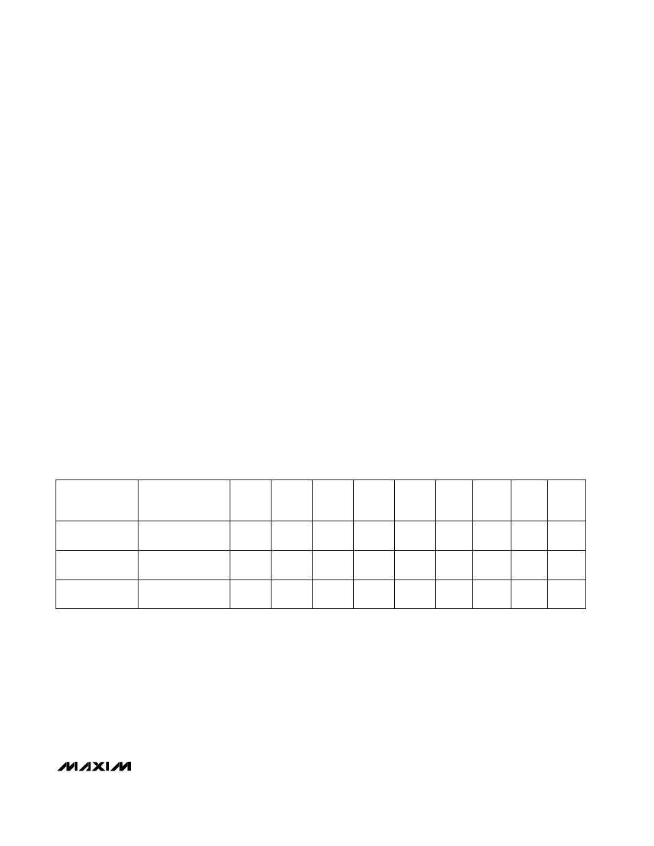
Table 1. Suggested Component Values for Discrete Lowpass Filters (0.1dB Ripple
Chebyshev Type)
Note:
Suggested types: Inductors: Coilcraft 1008CS, tolerance = ±5%; Capacitors: use tolerance = ±2%. Refer to Figure 2 for circuit
diagram.
0.1dB Chebyshev,
f
C
= 20MHz
40
0.1dB Chebyshev,
f
C
= 30MHz
60
0.1dB Chebyshev,
f
C
= 45MHz
90
ADC
SAMPLING
RATE (Msps)
FILTER
TYPE
100
100
100
R
S
(
Ω
)
39
22
18
C1
(pF)
910
620
390
L1
(nH)
120
82
56
C2
(pF)
1500
910
620
L2
(nH)
150
100
68
C3
(pF)
1500
1000
680
L3
(nH)
120
82
56
C4
(pF)
10
10
10
R
L
(k
Ω
)
