Ac electrical characteristics, Lm32 – Rainbow Electronics LM32 User Manual
Page 5
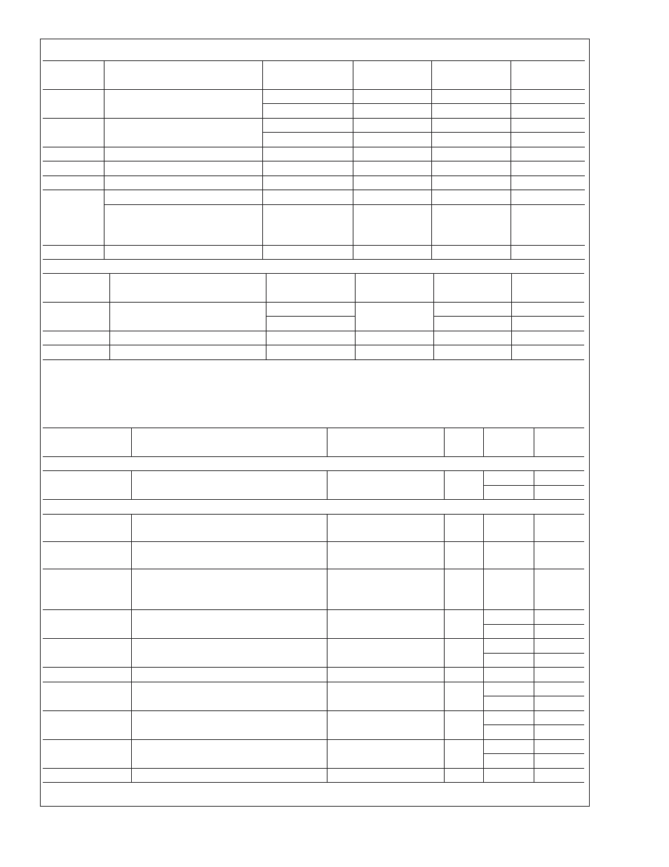
SWD and ADD DIGITAL INPUT CHARACTERISTICS
Symbol
Parameter
Conditions
Typical
Limits
Units
(Limit)
V
IH
SWD Logical High Input Voltage
2.1
V (min)
V+ + 0.5
V (max)
V
IL
SWD Logical Low Input Voltage
0.8
V (max)
-0.5
V (min)
V
IH
ADD Logical High Input Voltage
90% x V+
V (min)
V
IL
ADD Logical Low Input Voltage
10% x V+
V (max)
V
HYST
Input Hysteresis
300
mV
I
L
SWD and ADD Input Current
GND
≤ V
IN
≤ V+
±
0.005
±
10
µA (max)
SWD Input Current with V+ Open or
Grounded
GND
≤ V
IN
≤ 3.6V,
and V+ Open or
GND
±
0.005
µA
C
IN
Digital Input Capacitance
10
pF
SWD DIGITAL OUTPUT CHARACTERISTICS
Symbol
Parameter
Conditions
Typical
Limits
Units
(Limit)
V
OL
Open-drain Output Logic “Low”
Voltage
I
OL
= 4mA
0.4
V (max)
I
OL
= 50µA
0.2
V (max)
I
OH
Open-drain Output Off Current
±
0.005
±
10
µA (max)
C
OUT
Digital Output Capacitance
10
pF
AC Electrical Characteristics
The following specification apply for V+ = +3.0 V
DC
to +3.6 V
DC
, unless otherwise specified. Boldface limits apply for
T
A
= T
J
= T
MIN
=0˚C to T
MAX
=85˚C; all other limits T
A
= T
J
= 25˚C. The SensorPath Characteristics conform to the SensorPath
specification revision 0.98. Please refer to that speciation for further details.
Symbol
Parameter
Conditions
Typical
Limits
Units
(Limits)
HARDWARE MONITOR CHARACTERISTICS
t
CONV
Total Monitoring Cycle Time (Note 12)
All Temperature readings
(Default)
182
163.8
ms (min)
200.2
ms (max)
SensorPath Bus CHARACTERISTICS
t
f
SWD fall time (Note 15)
R
pull-up
=1.25 k
Ω
±
30%,
C
L
=400 pF
300
ns (max)
t
r
SWD rise time (Note 15)
R
pull-up
=1.25 k
Ω
±
30%,
C
L
=400 pF
1000
ns (max)
t
INACT
Minimum inactive time (bus at high level)
guaranteed by the slave before an attention
request
11
µs (min)
t
Mtr0
Master drive for Data Bit 0 write and for Data
Bit 0-1read
11.8
µs (min)
17.0
µs (max)
t
Mtr1
Master drive for Data Bit 1 write
35.4
µs (min)
48.9
µs (max)
t
SFEdet
Time allowed for LM32 activity detection
9.6
µs (max)
t
SLout1
LM32 drive for Data Bit 1 read by master
28.3
µs (min)
38.3
µs (max)
t
MtrS
Master drive for Start Bit
80
µs (min)
109
µs (max)
t
SLoutA
LM32 drive for Attention Request
165
µs (min)
228
µs (max)
t
RST
Master or LM32 drive for Reset
354
µs (min)
LM32
www.national.com
5