Timing characteristics (continued) – Rainbow Electronics MAX1092 User Manual
Page 5

MAX1090/MAX1092
400ksps, +5V, 8-/4-Channel, 10-Bit ADCs
with +2.5V Reference and Parallel Interface
_______________________________________________________________________________________
5
Note 1: Tested at V
DD
= +5V, COM = GND, unipolar single-ended input mode.
Note 2: Relative accuracy is the deviation of the analog value at any code from its theoretical value after offset and gain errors have
been removed.
Note 3: Offset nulled.
Note 4: On channel is grounded; sine wave applied to off channels.
Note 5: Conversion time is defined as the number of clock cycles times the clock period; clock has 50% duty cycle.
Note 6: Input voltage range referenced to negative input. The absolute range for the analog inputs is from GND to V
DD
.
Note 7: External load should not change during conversion for specified accuracy.
Note 8: When bit 5 is set low for internal acquisition, WR must not return low until after the first falling clock edge of the conversion.
TIMING CHARACTERISTICS (continued)
(V
DD
= V
LOGIC
= +5V ±10%, COM = GND, REFADJ = V
DD
, V
REF
= +2.5V, 4.7µF capacitor at REF pin, f
CLK
= 7.6MHz (50% duty
cycle), T
A
= T
MIN
to T
MAX
, unless otherwise noted. Typical values are at T
A
= +25°C.)
3k
3k
DOUT
DOUT
V
LOGIC
a) HIGH-Z TO V
OH
AND V
OL
TO V
OH
b) HIGH-Z TO V
OL
AND V
OH
TO V
OL
C
LOAD
20pF
C
LOAD
20pF
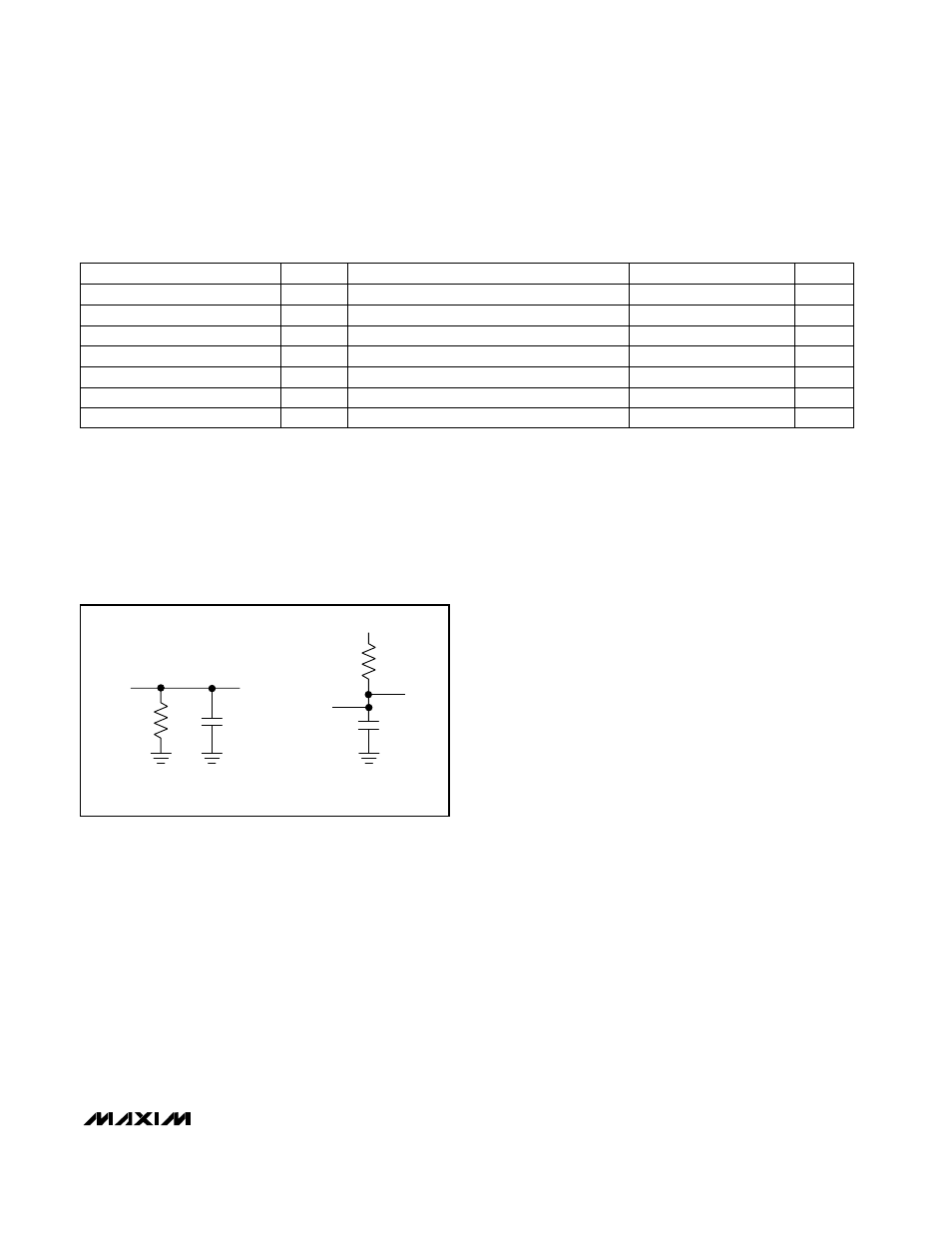
Figure 1. Load Circuits for Enable/Disable Times
t
TR
10
40
ns
C
LOAD
= 20pF, Figure 1
RD Rise to Output Disable
RD Fall to Output Data Valid
t
DO
10
50
ns
RD Fall to INT High Delay
t
INT1
50
ns
CS Fall to Output Data Valid
t
DO2
100
ns
C
LOAD
= 20pF, Figure 1
C
LOAD
= 20pF, Figure 1
C
LOAD
= 20pF, Figure 1
t
TC
10
60
ns
C
LOAD
= 20pF, Figure 1
PARAMETER
SYMBOL
MIN
TYP
MAX
UNITS
CONDITIONS
CS Rise to Output Disable
HBEN Rise to Output Data Valid
t
DO1
10
50
ns
C
LOAD
= 20pF, Figure 1
HBEN Fall to Output Data Valid
t
DO1
10
80
ns
C
LOAD
= 20pF, Figure 1
