Max2659 gps/gnss low-noise amplifier, Ac electrical characteristics – Rainbow Electronics MAX2659 User Manual
Page 2
MAX2659
GPS/GNSS Low-Noise Amplifier
2
_______________________________________________________________________________________
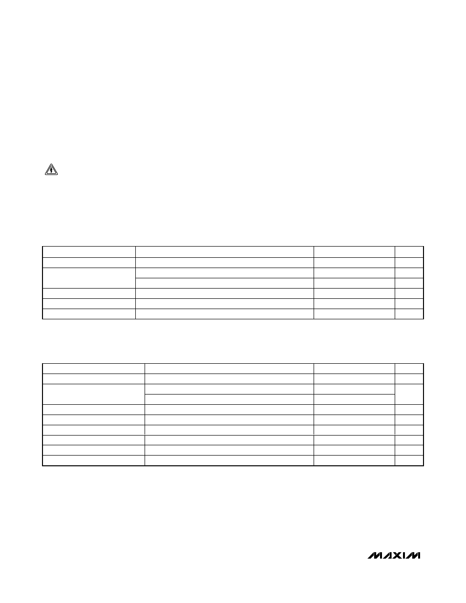
ABSOLUTE MAXIMUM RATINGS
DC ELECTRICAL CHARACTERISTICS
(MAX2659 EV kit; V
CC
= 1.6V to 3.3V, T
A
= -40°C to +85°C, no RF signals are applied. Typical values are at V
CC
= 2.85V and
T
A
= +25°C, unless otherwise noted.) (Note 1)
Stresses beyond those listed under “Absolute Maximum Ratings” may cause permanent damage to the device. These are stress ratings only, and functional
operation of the device at these or any other conditions beyond those indicated in the operational sections of the specifications is not implied. Exposure to
absolute maximum rating conditions for extended periods may affect device reliability.
Note 1: Min and Max limits guaranteed by test at T
A
= +25°C and guaranteed by design and characterization at T
A
= -40°C and
T
A
= +85°C.
Note 2: Guaranteed by design and characterization.
Note 3: Measured with the two tones located at 5MHz and 10MHz offset from the center of the GPS band with -40dBm/tone.
Note 4: Measured with a tone located at 5MHz offset from the center of the GPS band.
V
CC
to GND ...........................................................-0.3V to +4.2V
Other Pins to GND....................-0.3V to + Operating V
CC
+ 0.3V
Maximum RF Input Power .............................................+10dBm
Continuous Power Dissipation (T
A
= +70°C)
6-Pin µDFN (derates 2.1mW/°C above +70°C)............167mW
Operating Temperature Range ...........................-40°C to +85°C
Junction Temperature ......................................................+150°C
Storage Temperature Range .............................-65°C to +160°C
Lead Temperature (soldering, 10s) .................................+260°C
PARAMETER
CONDITIONS
MIN
TYP
MAX
UNITS
Supply
Voltage
1.6 2.85 3.3 V
SHDN = high
4.1
5.6
mA
Supply Current
Shutdown mode,
SHDN = low
1
µA
Digital Input-Logic High
1.4
V
Digital Input-Logic Low
0.4
V
Digital Input Current
1
µA
AC ELECTRICAL CHARACTERISTICS
(MAX2659 EV kit; V
CC
= 1.6V to 3.3V, T
A
= -40°C to +85°C, f
RFIN
= 1575.42MHz. Typical values are at V
CC
= 2.85V and T
A
= +25°C,
unless otherwise noted.) (Note 1)
PARAMETER
CONDITIONS
MIN
TYP
MAX
UNITS
RF Frequency
L1 band
1575.42
MHz
V
CC
= 2.85V
17
20.5
Power Gain
V
CC
= 1.6V
16.5
20.5
dB
Noise Figure
(Note 2)
0.8
dB
3rd-Order Input Intercept Point
(Note 3)
-5
dBm
Input 1dB Compression point
(Note 4)
-12
dBm
Input Return Loss
(Note 2)
10
15
dB
Output Return Loss
(Note 2)
10
25
dB
Reverse Isolation
(Note 2)
32
dB
CAUTION! ESD SENSITIVE DEVICE