Electrical characteristics (continued), Timing characteristics – Rainbow Electronics MAX1621 User Manual
Page 3
MAX1620/MAX1621
Digitally Adjustable LCD Bias Supplies
_______________________________________________________________________________________
3
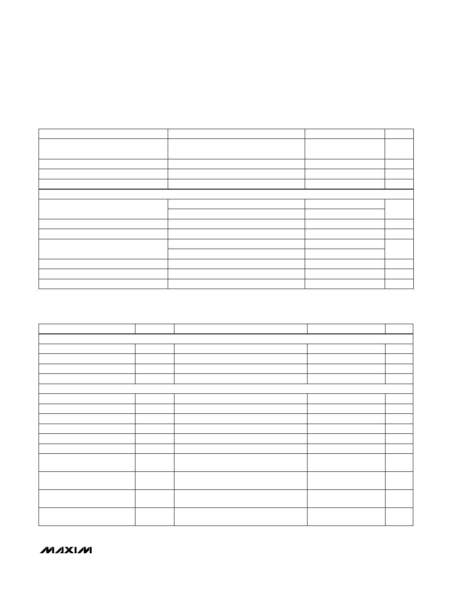
ELECTRICAL CHARACTERISTICS (continued)
(V
DD
= 3.3V, V
BATT
= 10V,
T
A
= 0°C to +85°C
, unless otherwise noted.)
TIMING CHARACTERISTICS
(
T
A
= 0°C to +85°C
, unless otherwise noted.)
-20µA
≤
I
DOUT
≤
0µA
I
SDA
= -6mA
V
IN
= 0V or V
IN
= V
DD
V
DD
= 5.5V
V
DD
= 5.5V
3.0V
≤
V
DD
≤
3.6V
3.0V
≤
V
DD
≤
3.6V
48.39mV step size
V
IN
= 0V or V
IN
= V
DD
Guaranteed monotonic
0µA
≤
I
DOUT
≤
40µA
V
0.4
µA
±1
SCL, SDA, SUS Input Leakage Current
V
0.6
SCL, SDA, SUS Input Low Voltage
V
2.3
1.4
SCL, SDA, SUS Input High Voltage
±1
V
0.6
V
0
0.007
DOUT Minimum Output Voltage (Note 3)
2.3
V
1.4
UP, DN, SHDN, POL Input High Voltage
LSB
DOUT Differential Nonlinearity
Bits
5
DOUT Resolution
±1
REF -
REF +
0.02
0.02
DOUT Maximum Output Voltage (Note 3)
V
UP, DN, SHDN, POL Input Leakage Current
µA
UP, DN, SHDN, POL Input Low Voltage
SDA Output Low Voltage
CONDITIONS
UNITS
MIN
TYP
MAX
PARAMETER
DIGITAL INPUTS AND OUTPUTS
(Note 4)
(Note 4)
(Note 4)
CONDITIONS
1
SCL Falling Edge to SDA Valid
Master Clocking in Data
µs
t
DV
µs
4
t
HD:STA
Start Condition SDA to SCL
Hold Time
µs
4.7
t
SU:STA
Start Condition SCL to SDA
Setup Time
µs
4
t
HIGH
SCL High Time
µs
4.7
t
LOW
SCL Low Time
ns
300
t
F
SCL/SDA Fall Time
µs
1
t
1
Pulse Width High (UP, DN)
µs
1
t
R
SCL/SDA Rise Time
ns
0
t
HD:DAT
SCL to SDA Data-Hold Time
ns
500
t
SU
:
DAT
SDA to SCL Data-Setup Time
µs
1
t
2
Pulse Width Low (UP, DN)
µs
1
t
3
Pulse Separation (UP, DN)
µs
1
t
4
Counter Reset Time
UNITS
MIN
TYP
MAX
SYMBOL
PARAMETER
µs
4
t
SU:STO
Stop Condition SCL_ to SDA_
Setup Time
MAX1620
(Figure 1)
MAX1621
(Figures 2 and 3)