Design procedure __________and component selection – Rainbow Electronics MAX1621 User Manual
Page 15
MAX1620/MAX1621
Digitally Adjustable LCD Bias Supplies
______________________________________________________________________________________
15
START
CONDITION
MOST
SIGNIFICANT
ADDRESS BIT
LEAST
SIGNIFICANT
ADDRESS BIT
SLAVE PULLS
SDA LOW
MAX1621 DRIVES SDA
D4
POK
D3
D2
D1
D0
SLAVE
ACKNOWLEDGE
MOST
SIGNIFICANT
DATA BIT
SCL
SDA
R/W BIT
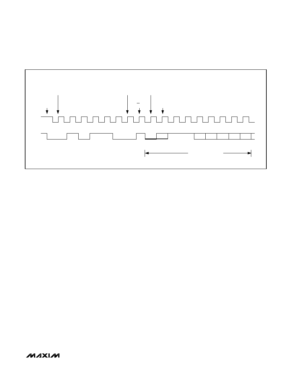
Figure 9. MAX1621 Serial-Interface Read Example
Design Procedure
__________and Component Selection
The MAX1620/MAX1621 output voltage can be adjusted
manually or via a digital interface. In addition, positive
bias voltage can be switched with LCDON using an
external PFET or PNP transistor.
Output Adjustment
Setting the Minimum Output Voltage
The minimum output voltage is set with a resistor-divider
(R4-R5, Figure 4) from V
OUT
to AGND. The FB threshold
voltage is 1.5V. Choose R4 to be 300k
Ω
so that the cur-
rent in the divider is about 5µA. Determine R5 as follows:
R5 = R4 x (V
OUT,MIN
- V
FB
) / V
FB
For example, if V
OUT,MIN
= 12.5V:
R5 = 300k
Ω
x (12.5 - 1.5) / (1.5) = 2.2M
Ω
Mount R4 and R5 close to the FB pin to minimize para-
sitic capacitance.
For a negative output voltage, the FB threshold voltage
is 0V, and R4 is placed between FB and REF (Figures 5
and 6). Again, choose R4 to be 300k
Ω
so that the cur-
rent in the divider is about 5µA. Then determine R5 as
follows:
R5 = R4 x
V
OUT,MIN
/ V
REF
For example, if V
OUT,MIN
= -12.5V:
R5 = 300k
Ω
x
(12.5) / (1.5)
= 2.5M
Ω