Rainbow Electronics MAX1289 User Manual
Page 9

MAX1286–MAX1289
150ksps, 12-Bit, 2-Channel Single-Ended, and
1-Channel True-Differential ADCs in SOT23
_______________________________________________________________________________________
9
Analog Input Protection
Internal protection diodes that clamp the analog input to
V
DD
and GND allow the analog input pins to swing from
GND - 0.3V to V
DD
+ 0.3V without damage. Both inputs
must not exceed V
DD
by more than 50mV or be lower
than GND by more than 50mV for accurate conversions.
If an off-channel analog input voltage exceeds the
supplies, limit the input current to 2mA.
Internal Clock
The MAX1286–MAX1289 operate from an internal oscilla-
tor, which is accurate within 10% of the 4MHz specified
clock rate. This results in a worst-case conversion time of
3.7µs. The internal clock releases the system micro-
processor from running the SAR conversion clock and
allows the conversion results to be read back at the
processor’s convenience, at any clock rate from 0 to
8MHz.
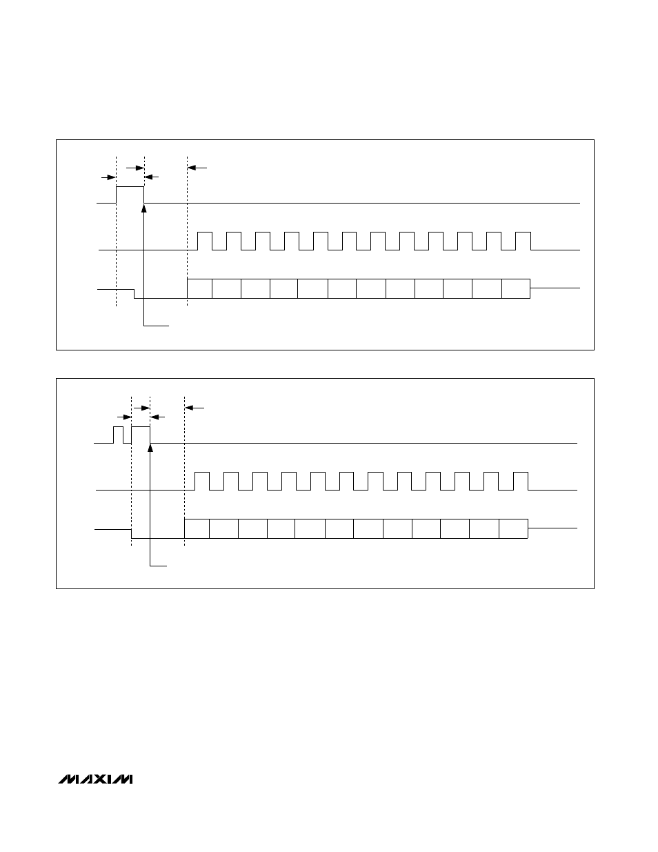
CNVST
SCLK
DOUT
t
ACQ
t
CONV
SAMPLING INSTANT
4
1
8
12
B11
MSB
B10
B9
B8
B7
B6
B5
B4
B3
B2
B1
B0
LSB
HIGH-Z
HIGH-Z
CNVST
SCLK
DOUT
t
ACQ
t
CONV
SAMPLING INSTANT
4
1
8
12
B11
MSB
B10
B9
B8
B7
B6
B5
B4
B3
B2
B1
B0
LSB
HIGH-Z
HIGH-Z
Figure 5b. Single Conversion AIN2 vs. GND (MAX1286/MAX1287), Bipolar Mode AIN+ vs. AIN- (MAX1288/MAX1289)
Figure 5a. Single Conversion AIN1 vs. GND (MAX1286/MAX1287), Unipolar Mode AIN+ vs. AIN- (MAX1288/MAX1289)
