Max2690, Low-noise, 2.5ghz downconverter mixer, Applications information – Rainbow Electronics MAX2690 User Manual
Page 8: Layout issues, Table 1. rf input impedance
MAX2690
__________Applications Information
Local-Oscillator (LO) Input
The LO input is a single-ended broadband 50
Ω
input with
a return loss of better than 10dB from 900MHz to 3GHz,
improving at high frequency. For lower-frequency LO
operation, a shunt resistor can be used to improve the LO
port match (see the
Typical Operating Circuit
for more
information). AC couple to LO. The LO signal is mixed
with the input RF signal, and the resulting downconverted
output appears on the IFOUT+ and IFOUT- pins.
RF Input
The typical RF input frequency range is 400MHz to
2.5GHz. For optimum performance, the RF input requires
an impedance-matching network. Consult Table 1 as well
as the RF Port Impedance vs. Frequency graph in the
Typical Operating Characteristics
.
IF Output
The IF output frequency range is typically 10MHz to
500MHz. The IFOUT+ and IFOUT- pins require external
inductors to V
CC
for proper biasing. These outputs are
high-impedance open collectors. In many applications,
the biasing inductors have resistors in parallel with
them to set an output impedance. Alternatively, a resis-
tor between IFOUT+ and IFOUT- may be used. Consult
the
Typical Operating Characteristics
section for more
information.
For single-ended operation, the IFOUT- pin can be tied
directly to V
CC
.
Power Supply and Bypassing
Proper attention to supply bypassing is essential for a
high-frequency RF circuit. V
CC
(pin 5) must be properly
bypassed with a 0.1µF capacitor in parallel with
1000pF to ground. Separate vias to the ground plane
are needed for each of the bypass capacitors, as well
as minimal trace length to reduce inductance. Each
ground pin should have a separate via to the ground
plane. Low-inductance ground connections and con-
trolled-impedance lines should be used in the layout.
To minimize noise on the internal bias cell, SHDN
should be decoupled with a 1000pF capacitor to
ground. A series resistor (typically 100
Ω
) can also be
used to reduce high-frequency signals coupling into
the SHDN pin.
Inductive Degeneration Pin (LGND)
A series inductor is typically connected from LGND to
GND. Adjusting the value of this inductor allows the
MAX2690 to be set to the optimum gain and linearity
point for a particular application. A short from LGND to
ground provides maximum linearity. Increasing the induc-
tor value trades off linearity for gain. A large inductor pro-
vides maximum gain. See the
Typical Operating
Characteristics
for a graph of conversion gain and lineari-
ty for several inductor values. The inductor’s self-resonant
frequency (SRF) should be as close as possible to or
above the desired RF frequency for optimal performance.
______________________Layout Issues
A well-designed PC board is an essential part of an RF
circuit. For best performance, pay attention to power-
supply issues as well as the layout of the RFIN match-
ing network.
Power-Supply Layout
To minimize coupling between different sections of the
IC, the ideal power-supply layout is a star configuration,
which has a large decoupling capacitor at a central
V
CC
node. The V
CC
traces branch out from this node,
each going to a separate V
CC
node in the MAX2690
circuit. At the end of each of these traces is a bypass
capacitor that is good at the RF frequency of interest.
This arrangement provides local decoupling at each
V
CC
pin. At high frequencies, any signal leaking out
one supply pin sees a relatively high impedance
(formed by the V
CC
trace inductance) to the central
V
CC
node, and an even higher impedance to any other
supply pin, as well as a low impedance to ground.
Matching-Network Layout
The layout of the RFIN matching network can be very
sensitive to parasitic circuit elements. To minimize par-
asitic inductance, keep all traces short, and place com-
ponents as close to the chip as possible. To minimize
parasitic capacitance, a cut-out in the ground plane
(and any other planes) below the matching network
components can be used.
Low-Noise, 2.5GHz
Downconverter Mixer
8
_______________________________________________________________________________________
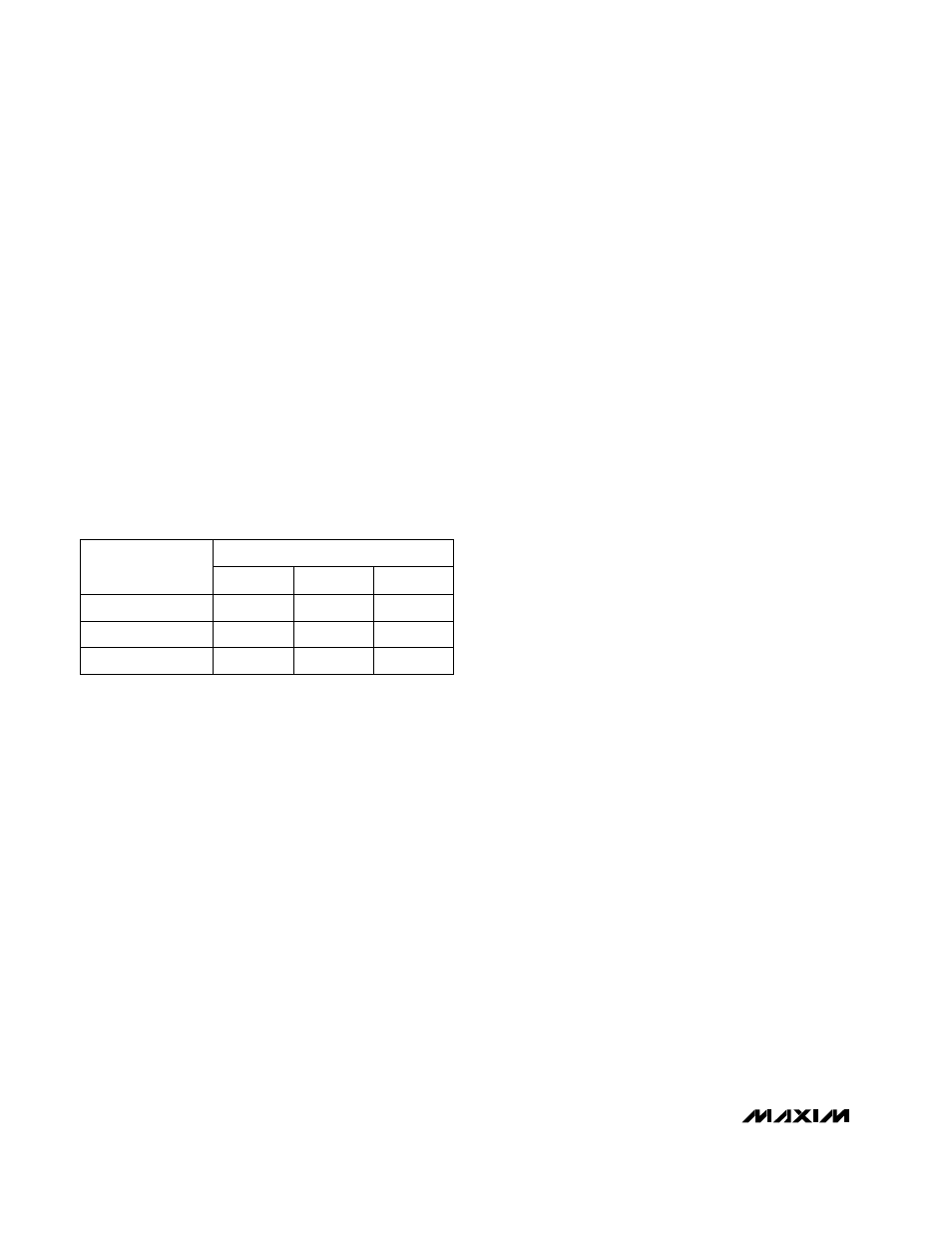
Table 1. RF Input Impedance
630
Ω
20 – j 110
Ω
400
Ω
18 – j 85
Ω
1100
Ω
Equivalent Shunt R
45 – j 219
Ω
Series Z
PART
FREQUENCY
0.7pF
0.7pF
0.7pF
Equivalent Shunt C
1.95GHz
2.45GHz
900MHz