Transfer function, Layout, grounding, and bypassing – Rainbow Electronics MAX1081 User Manual
Page 19
MAX1080/MAX1081
300ksps/400ksps, Single-Supply, Low-Power,
8-Channel, Serial 10-Bit ADCs with Internal Reference
______________________________________________________________________________________
19
External Reference
An external reference can be placed at the input
(REFADJ) or the output (REF) of the internal reference-
buffer amplifier. The REFADJ input impedance is typi-
cally 17k
Ω. At REF, the DC input resistance is a
minimum of 18k
Ω. During conversion, an external refer-
ence at REF must deliver up to 350µA DC load current
and have 10
Ω or less output impedance. If the refer-
ence has a higher output impedance or is noisy, bypass
it close to the REF pin with a 4.7µF capacitor.
Using the REFADJ input makes buffering the external
reference unnecessary. To use the direct REF input,
disable the internal buffer by connecting REFADJ to
V
DD1
.
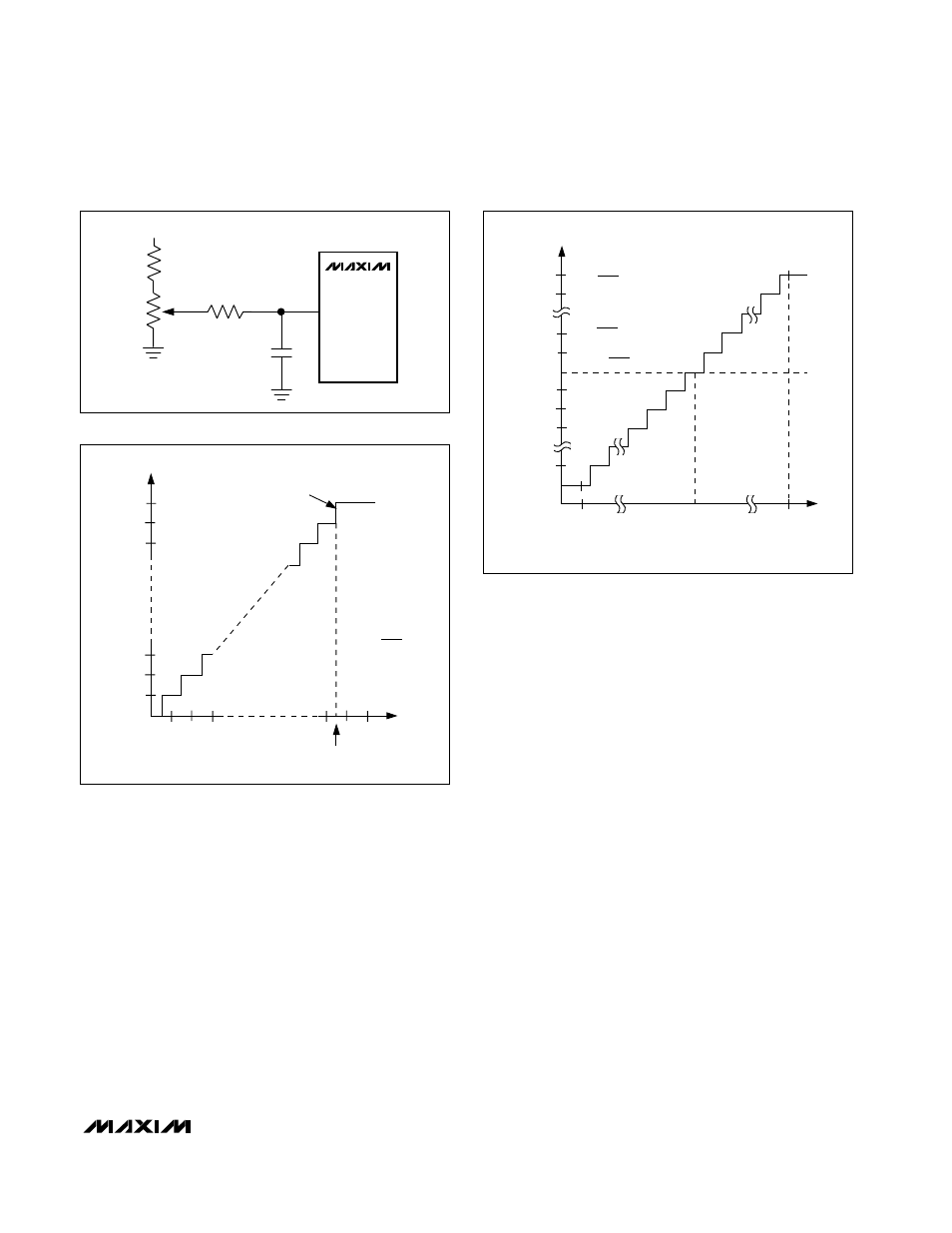
Transfer Function
Table 5 shows the full-scale voltage ranges for unipolar
and bipolar modes. Figure 14 depicts the nominal,
unipolar input/output (I/O) transfer function, and Figure
15 shows the bipolar I/O transfer function. Code transi-
tions occur halfway between successive-integer LSB
values. Output coding is binary, with 1LSB = 2.44mV
for unipolar and bipolar operation.
Layout, Grounding, and Bypassing
For best performance, use PC boards; wire-wrap boards
are not recommended. Board layout should ensure that
digital and analog signal lines are separated from each
other. Do not run analog and digital (especially clock)
lines parallel to one another, or digital lines underneath
the ADC package.
Figure 16 shows the recommended system ground
connections. Establish a single-point analog ground
(star ground point) at GND. Connect all other analog
grounds to the star ground. Connect the digital system
ground to this ground only at this point. For lowest-
noise operation, the ground return to the star ground’s
power supply should be low impedance and as short
as possible.
High-frequency noise in the V
DD1
power supply may
affect the high-speed comparator in the ADC. Bypass
the supply to the star ground with 0.1µF and 10µF
capacitors close to pin 20 of the MAX1080/MAX1081.
+3.3V
510k
24k
100k
0.01
µF
12
REFADJ
MAX1081
Figure 13. MAX1081 Reference-Adjust Circuit
OUTPUT CODE
FULL-SCALE
TRANSITION
11 . . . 111
11 . . . 110
11 . . . 101
00 . . . 011
00 . . . 010
00 . . . 001
00 . . . 000
1
2
3
0
(COM)
FS
FS - 3/2LSB
FS = V
REF
+ V
COM
ZS = V
COM
INPUT VOLTAGE (LSB)
1LSB =
V
REF
1024
Figure 14. Unipolar Transfer Function, Full Scale (FS) = V
REF
+ V
COM
, Zero Scale (ZS) = V
COM
011 . . . 111
011 . . . 110
000 . . . 010
000 . . . 001
000 . . . 000
111 . . . 111
111 . . . 110
111 . . . 101
100 . . . 001
100 . . . 000
- FS
COM*
INPUT VOLTAGE (LSB)
OUTPUT CODE
ZS = V
COM
+FS - 1LSB
*V
COM
V
REF
/ 2
+ V
COM
FS
=
V
REF
2
-FS =
+ V
COM
-V
REF
2
1LSB =
V
REF
1024
≤
Figure 15. Bipolar Transfer Function, Full Scale (FS) =
V
REF
/ 2 + V
COM
, Zero Scale (ZS) = V
COM