Rainbow Electronics MAX1081 User Manual
Page 13
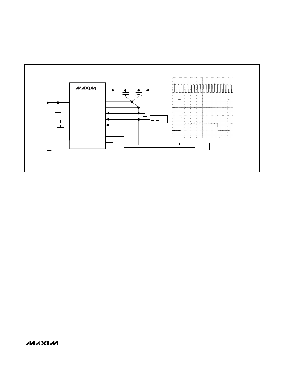
Quick Look
To quickly evaluate the MAX1080/MAX1081s’ analog per-
formance, use the circuit of Figure 5. The devices require
a control byte to be written to DIN before each conver-
sion. Connecting DIN to V
DD2
feeds in control bytes of
$FF (HEX), which trigger single-ended unipolar conver-
sions on CH7 without powering down between conver-
sions. The SSTRB output pulses high for one clock
period before the MSB of the conversion result is shift-
ed out of DOUT. Varying the analog input to CH7 will
alter the sequence of bits from DOUT. A total of 16
clock cycles is required per conversion. All transitions
of the SSTRB and DOUT outputs typically occur 20ns
after the rising edge of SCLK.
Starting a Conversion
Start a conversion by clocking a control byte into DIN.
With CS low, each rising edge on SCLK clocks a bit from
DIN into the MAX1080/MAX1081s’ internal shift register.
After CS falls, the first arriving logic “1” bit defines the
control byte’s MSB. Until this first “start” bit arrives, any
number of logic “0” bits can be clocked into DIN with no
effect. Table 3 shows the control-byte format.
The MAX1080/MAX1081 are compatible with SPI/
QSPI and MICROWIRE devices. For SPI, select the cor-
rect clock polarity and sampling edge in the SPI control
registers: set CPOL = 0 and CPHA = 0. MICROWIRE,
SPI, and QSPI all transmit a byte and receive a byte at
the same time. Using the Typical Operating Circuit, the
simplest software interface requires only three 8-bit
transfers to perform a conversion (one 8-bit transfer to
configure the ADC, and two more 8-bit transfers to clock
out the conversion result). See Figure 17 for MAX1080/
MAX1081 QSPI connections.
Simple Software Interface
Make sure the CPU’s serial interface runs in master
mode so the CPU generates the serial clock. Choose a
clock frequency from 500kHz to 6.4MHz (MAX1080) or
4.8MHz (MAX1081):
1) Set up the control byte and call it TB1. TB1 should
be of the format: 1XXXXXXX binary, where the Xs
denote the particular channel, selected conversion
mode, and power mode.
2) Use a general-purpose I/O line on the CPU to pull
CS low.
3) Transmit TB1 and simultaneously receive a byte
and call it RB1. Ignore RB1.
4) Transmit a byte of all zeros ($00 hex) and simulta-
neously receive byte RB2.
5) Transmit a byte of all zeros ($00 hex) and simulta-
neously receive byte RB3.
6) Pull CS high.
MAX1080/MAX1081
300ksps/400ksps, Single-Supply, Low-Power,
8-Channel, Serial 10-Bit ADCs with Internal Reference
______________________________________________________________________________________
13
10
µF
0.1
µF
2.5V
V
DD1
V
DD2
GND
COM
CS
SCLK
DIN
DOUT
SSTRB
SHDN
V
DD2
V
DD2
0.01
µF
0.01
µF
CH7
REFADJ
REF
4.7
µF
0 TO
+2.500V
ANALOG
INPUT
OSCILLOSCOPE
CH1
CH2
CH3
CH4
*FULL-SCALE ANALOG INPUT, CONVERSION RESULT = $3FF (HEX)
MAX1080
MAX1081
+3V OR +5V
EXTERNAL CLOCK
SCLK
SSTRB
DOUT*
Figure 5. Quick-Look Circuit