Detailed description, Device operation, Table 1. potentiometer registers – Rainbow Electronics DS3903 User Manual
Page 7

Detailed Description
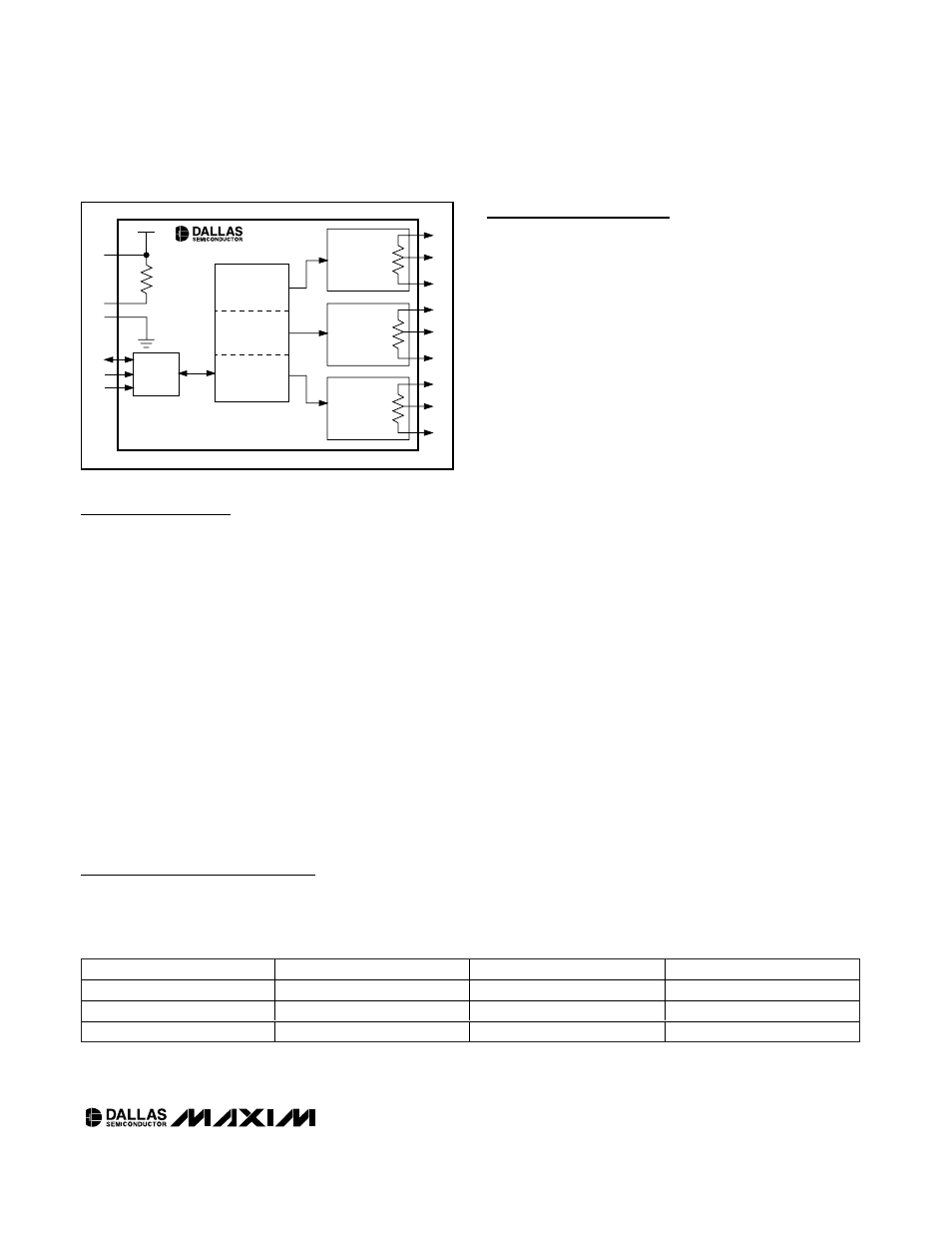
The DS3903 contains three NV, low-temperature coeffi-
cient digital potentiometers. It is accessible through a
2-wire bus, and it serves as a small, low-cost replace-
ment for designs using mechanical potentiometers. The
low end-to-end resistance temperature coefficient is
especially beneficial for designs using a digital poten-
tiometer as a 2-terminal variable resistor.
It operates in both 3V and 5V systems, and it features a
write-protect pin that can lock the positions of the
potentiometers. The address pin allows two DS3903s to
be placed on the same 2-wire bus.
With its low cost and small board space, the DS3903 is
well tailored to replace larger mechanical potentiome-
ters. This allows the automation of calibration in many
instances because the 2-wire interface can easily be
adjusted by test hardware. Once the system is calibrat-
ed, the write-protect pin can be disconnected and the
potentiometers retain their settings.
Potentiometer Memory
Organization
The potentiometers of the DS3903 are addressed by
communicating with the registers in Table 1.
Device Operation
Clock and Data Transitions
The SDA pin is normally pulled high with an external
resistor or device. Data on the SDA pin can only change
during SCL low time periods. Data changes during SCL
high periods indicates a start or stop condition depend-
ing on the conditions discussed below. See the timing
diagrams for further details (Figures 2 and 3).
Start Condition
A high-to-low transition of SDA with SCL high is a start
condition, which must precede any other command. See
the timing diagrams for further details (Figures 2 and 3).
Stop Condition
A low-to-high transition of SDA with SCL high is a stop
condition. After a read sequence, the stop command
places the DS3903 into a low-power mode. See the tim-
ing diagrams for further details (Figures 2 and 3).
Acknowledge
All address and data bytes are transmitted through a
serial protocol. The DS3903 pulls the SDA line low dur-
ing the ninth clock pulse to acknowledge that it has
received each word.
Standby Mode
The DS3903 features a low-power mode that is auto-
matically enabled after power-on, after a stop com-
mand, and after the completion of all internal
operations.
Memory Reset
After any interruption in protocol, power loss, or system
reset, the following steps reset the DS3903:
1)
Clock up to nine cycles.
2)
Look for SDA high in each cycle while SCL is high.
3)
Create a start condition while SDA is high.
Device Addressing
The DS3903 must receive an 8-bit device address word
following a start condition to enable a specific device
for a read or write operation. The address word is
clocked into the DS3903 MSB to LSB. The address
DS3903
Triple 128-Position Nonvolatile
Digital Potentiometer
_____________________________________________________________________
7
POTENTIOMETER 2
10k
Ω
ADDDR FAh
POTENTIOMETER 2
ADDDR FAh
2-WIRE
INTERFACE
EEPROM
DATA
RWP
WP
GND
SCL
SDA
A0
V
CC
V
CC
H2
W2
L2
POTENTIOMETER 0
10k
Ω
ADDDR F9h
POTENTIOMETER 0
ADDDR F9h
POTENTIOMETER 1
90k
Ω
ADDDR F8h
POTENTIOMETER 1
ADDDR F8h
H0
W0
L0
H1
W1
L1
DS3903
Figure 1. DS3903 Block Diagram
ADDRESS
POTENTIOMETER
END-TO-END RESISTANCE
NUMBER OF POSITIONS
F8h
Pot 1
90k
Ω
*128 (00h to 7Fh)
F9h
Pot 0
10k
Ω
*128 (00h to 7Fh)
FAh
Pot 2
10k
Ω
*128 (00h to 7Fh)
Table 1. Potentiometer Registers
*The most significant bit of each potentiometer position value is ignored. Writing a value greater than 7Fh to any of the potentiometer
registers results in a valid 7-bit position, without regard to the value of the most significant bit. Example: position 0x82 is the same as
position 0x02.
