Ds4432 dual-channel, i, C, 7-bit sink/source current dac, Detailed description – Rainbow Electronics DS4432 User Manual
Page 6: C serial interface description

DS4432
Dual-Channel, I
2
C, 7-Bit Sink/Source
Current DAC
6
_______________________________________________________________________________________
Detailed Description
The DS4432 contains two I
2
C adjustable current DACs
that are each capable of sinking and sourcing current.
Each output (OUT0 and OUT1) has 127 sink and 127
source settings that can be controlled by the I
2
C inter-
face. The full-scale ranges and corresponding step
sizes of the outputs are determined by external resis-
tors, connected to pins FS0 and FS1.
The formula to determine R
FS
(connected to the FSx
pins) to attain the desired full-scale current range is:
Equation 1:
where I
FS
is the desired full-scale current value, V
RFS
is
the R
FS
voltage (see the
DC Electrical Characteristics
table), and R
FS
is the external resistor value.
To calculate the output current value (I
OUT
) based on the
corresponding DAC value (see Table 1 for corresponding
memory addresses), use equation 2.
Equation 2:
On power-up the DS4432 outputs zero current. This is
done to prevent the device from sinking or sourcing an
incorrect amount of current before the system host con-
troller has had a chance to modify the DS4432’s setting.
As a source for biasing instrumentation or other circuits,
the DS4432 provides a simple and inexpensive current
DAC with an I
2
C interface for control. The adjustable
full-scale range allows the application to get the most
out of its 7-bit sink or source resolution.
When used in adjustable power-supply applications
(see the
Typical Operating Circuit
), the DS4432 does
not affect the initial power-up voltage of the supply
because it defaults to providing zero output current on
power-up. As the device sources or sinks current into
the feedback-voltage node, it changes the amount of
output voltage required by the regulator to reach its
steady-state operating point. Using the external resistor,
R
FS
, to set the output current range, the DS4432 pro-
vides some flexibility for adjusting the impedances of
the feedback network or the range over which the power
supply can be controlled or margined.
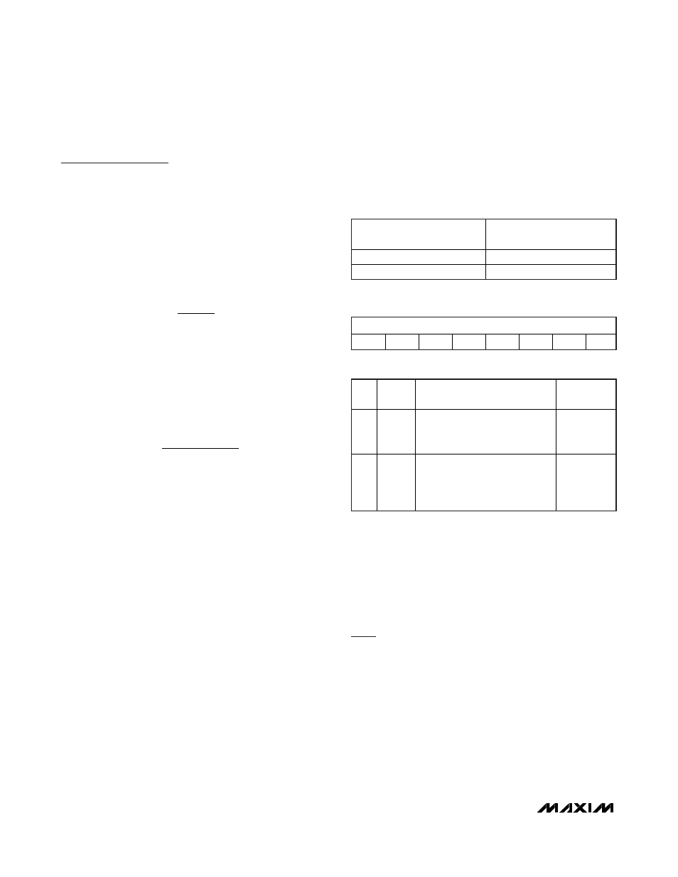
Memory Organization
To control the DS4432’s current sources, write to the
memory addresses listed in Table 1.
The format of each output control register is:
where:
Example: R
FS0
= 80k
Ω and register 0xF8h is written to
a value of 0xAAh. Calculate the output current.
I
FS
= (0.997V/80k
Ω) x (127/16) = 98.921µA
The MSB of the output register is 1, so the output is sourc-
ing the value corresponding to position 2Ah (42 decimal).
The magnitude of the output current is equal to:
98.921µA x (42/127) = 32.714µA
I
2
C Serial Interface Description
I
2
C Slave Address
The DS4432’s slave address is 90h.
I
2
C Definitions
The following terminology is commonly used to describe
I
2
C data transfers:
Master Device: The master device controls the slave
devices on the bus. The master device generates
SCL clock pulses and START and STOP conditions.
I
D
1
I
OUT
FS
=
×
AC Value dec
(
)
27
R
V
16
I
FS
RFS
FS
=
Ч
Ч 127
Table 1. Memory Addresses
MEMORY ADDRESS
(HEX)
CURRENT SOURCE
F8h OUT0
F9h OUT1
MSB
LSB
S D
6
D
5
D
4
D
3
D
2
D
1
D
0
BIT
NAME
FUNCTION
POWER-ON
DEFAULT
S
Sign
Bit
Determines if DAC sources or
sinks current. For sink
S = 0; for source S = 1.
0b
D
X
Data
7-Bit Data Controlling DAC
Output. Setting 0000000b
outputs zero current regardless
of the state of the sign bit.
0000000b
