Ba3131fs, Standard ics – Rainbow Electronics BA3131FS User Manual
Page 8

BA3131FS
Standard ICs
!
!
!
!Operation notes
(1) Pin 13 is the reference output pin, from which 1 / 2 Vcc is output. The value for the bypass capacitor should be
determined based on the desired characteristics. A value between 500pF and 1
µF may produce oscillation, so if AC
grounding is being used, always use a bypass capacitor with a value of at least 10
µF.
Also, Pin 12 is designated for reference circuit input, so if reference output is being used, always use a bypass capacitor
for AC grounding. (We recommend a bypass capacitor with a value of 22
µF.)
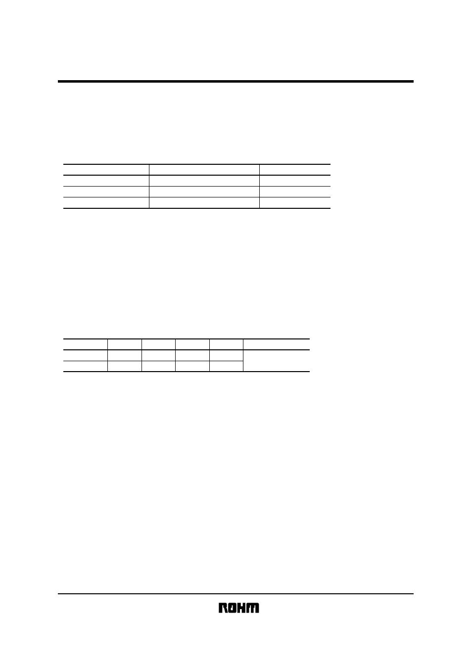
•Reference data (these values are intended only as a reference, and performance is not guaranteed)
10
– 35
150
22
– 42
300
47
– 48
550
Ripple rejection ratio (f
IN
= 100 Hz) (dB)
Pin 12 bypass capacitor (
µ
F)
Output rise time (ms)
∗
∗
Test conditions: When power supply is on (V
CC
= 8V), time equal to 90% of V
CC
bypass capacitor,Pin 13 bypass
capacitor 100
µ
F, output smoothing voltage.
(2) This IC offers stability even at low gain (0 to 20dB), but a capacitance load of 200pF or higher may cause oscillation
(the phase margin at a capacitance of 200pF is 10
° typ. (Ta = 85°C, 0dB point) ). Consequently, please make sure
sufficient care is taken in terms of the capacitance load.
When using a 0dB buffer, as shown in the application example (Figure 13), introducing a bias resistance of several k
Ω to
the negative input (R11 and R12 in Figure 13, indicated as circled items) results in greater stability in terms of the
capacitance load.
!
!
!
!Truth value table
H
H
Corresponds to
µ
COM output
ch1
Conditions
∗
“H” when the applied voltage at pins 8 and 9 is 2.0V or more, and “L” when it is 1.0V or less.
SW1 (8pin)
SW2 (9pin)
H
L
ch2
L
H
ch3
L
L
OFF
