Ba3131fs, Standard ics – Rainbow Electronics BA3131FS User Manual
Page 2

BA3131FS
Standard ICs
!
!
!
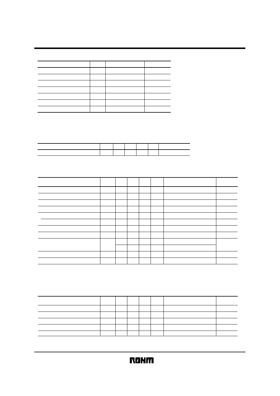
!Absolute maximum ratings
(Ta=25
°C)
Parameter
Symbol
Limits
Unit
Power supply voltage
V
Power dissipation
750
∗
mW
Operating temperature
Topr
˚C
Storage temperature
Tstg
˚C
Common-mode input voltage
V
Differential input voltage
V
Load current
± 50.0
mA
∗
Reduced by 7.5mW for each increase in Ta of 1˚C over 25˚C.
V
CC
3 ~ V
CC
V
CC
Vi
Vid
18.0
Pd
I
oMax.
– 40 ~ + 85
– 55 ~ + 125
(When mounted on a glass epoxy board (90mm
×
50mm
×
1.6t))
!
!
!
!Recommended operating conditions
(Ta=25
°C)
Parameter
Symbol Min.
Typ.
Max.
Unit
Conditions
Operating power supply voltage
V
CC
6.0
8.0
16.0
V
single power source
!
!
!
!Electrical characteristics
(unless otherwise noted, Ta=25
°C, Vcc=8V)
Parameter
Symbol
Min.
Typ.
Max.
Unit
Conditions
Quiescent current
2.0
4.9
7.8
mA
Input offset voltage
-
0.5
5.0
mV
Input offset current
-
5
200
nA
Input bias current
-
50
500
nA
High-amplitude voltage gain
86
110
-
dB
Common-mode input voltage
3
6
-
V
In-phase signal rejection ratio
CMRR
60
72
-
dB
Power supply voltage rejection ratio
PSRR
76
90
-
dB
Maximum output voltage
/
V
OH
V
OL
3
6
-
V
/
3
6
-
V
Input conversion noise voltage
-
2.0
4.0
µ
Vrms
Reference voltage change
-
-
± 10
mV
-
Iq
Vio
Iio
Ib
Vicm
Vn
RS
≤
10k
Ω
RL
≥
2k
Ω
, V
O
=
± 1.5V
RS
≤
10k
Ω
RS
≤
10k
Ω
RL
≥
10k
Ω
Ioref = ± 1mA
Fig.2
Fig.1
Fig.1
Fig.1
Fig.1
Fig.1
Fig.1
Fig.1
Fig.3
Fig.4
Fig.7
Avol
RL
≥
2k
Ω
∗
2
∗
1
V
IN
= 0, RL =
∞
, SW pin open
Measurement
circuit
∆
V
REF
∗
1 Because the first stage is contigured with PNP transistors, input bias current is from the IC.
∗
2 Tested under the following conditions: G
V
=
40dB, RS = 2k
Ω
, Matsushita Tsuko VP-9690A (using DIN audio filter)
!
!
!
!Design guaranteed values
(unless otherwise noted, Ta=25
°C, Vcc=8V)
Slew rate
SR
0.5
1.2
-
V /
µ
S
Gainbandwidth product
GBW
1.5
2.6
-
MHz
f = 10kHz
Crosstalk between A, B and C
CT
ABC
60
73
-
dB
f = 1kHz
THD
-
0.0025 0.01
%
CS
90
115
-
dB
Parameter
Symbol
Min.
Typ.
Max.
Unit
Conditions
Fig.5
Fig.6
Fig.8
Fig.9
Fig.10
Channel separation
∗
This item is not guaranteed during processes.
Total harmonic distortion
Measurement
circuit
f = 1kHz, input conversion
G
V
= 0dB, f = 1kHz, V
O
= 1Vrms
G
V
= 0dB, RL = 2k
Ω
