Pin descriptions and equivalent circuits – Rainbow Electronics ADC08100 User Manual
Page 3
Pin Descriptions and Equivalent Circuits
(Continued)
Pin No.
Symbol
Equivalent Circuit
Description
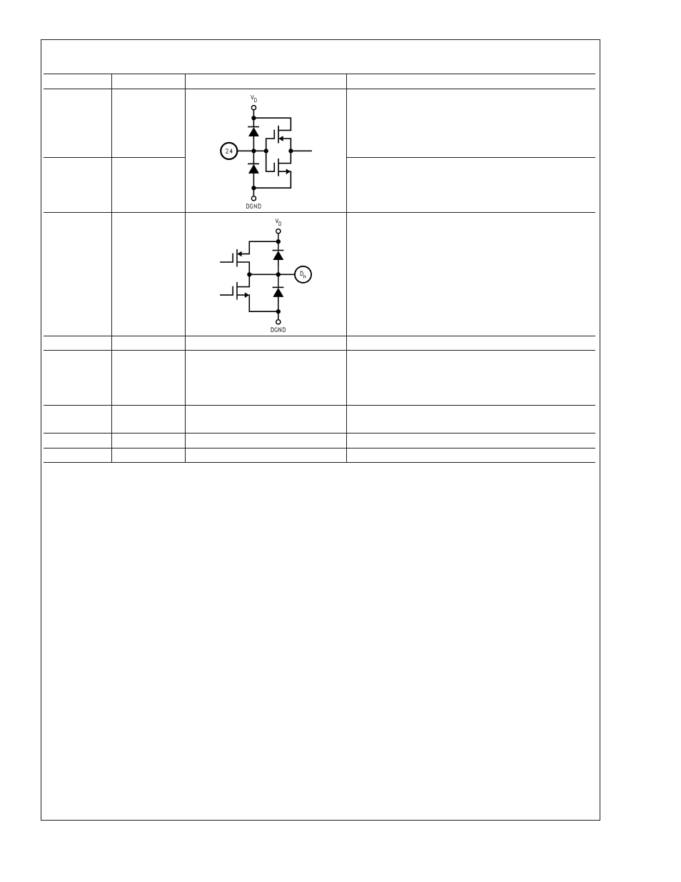
23
PD
Power Down input. When this pin is high, the converter is
in the Power Down mode and the data output pins hold
the last conversion result.
24
CLK
CMOS/TTL compatible digital clock Input. V
IN
is sampled
on the falling edge of CLK input.
13 thru 16
and
19 thru 22
D0–D7
Conversion data digital Output pins. D0 is the LSB, D7 is
the MSB. Valid data is output just after the rising edge of
the CLK input.
7
V
IN
GND
Reference ground for the single-ended analog input, V
IN
.
1, 4, 12
V
A
Positive analog supply pin. Connect to a clean, quiet
voltage source of +3V. V
A
should be bypassed with a
0.1 µF ceramic chip capacitor for each pin, plus one
10 µF capacitor. See Section 3.0 for more information.
18
DR V
D
Power supply for the output drivers. If connected to V
A
,
decouple well from V
A
.
17
DR GND
The ground return for the output driver supply.
2, 5, 8, 11
AGND
The ground return for the analog supply.
ADC08100
www.national.com
3