0 the analog input, Applications information – Rainbow Electronics ADC08100 User Manual
Page 15
Applications Information
(Continued)
V
RT
should always be at least 1.0V more positive than V
RB
to minimize noise.
The V
RM
pin is the center of the reference ladder and should
be bypassed to a clean, quiet point in the analog ground
plane with a 0.1 µF capacitor. DO NOT allow this pin to float.
2.0 THE ANALOG INPUT
The analog input of the ADC08100 is a switch followed by an
integrator. The input capacitance changes with the clock
level, appearing as 3 pF when the clock is low, and 4 pF
when the clock is high. The sampling nature of the analog
input causes current spikes at the input that result in voltage
spikes there. Any amplifier used to drive the analog input
must be able to settle within the clock high time. The
LMH6702 and the LMH6628 have been found to be good
amplifiers to drive the ADC08100.
Figure 4 shows an example of an input circuit using the
LMH6702. Any input amplifier should incorporate some gain
as operational amplifiers exhibit better phase margin and
transient response with gains above 2 or 3 than with unity
gain. If an overall gain of less than 3 is required, attenuate
the input and operate the amplifier at a higher gain, as
shown in Figure 4.
10137133
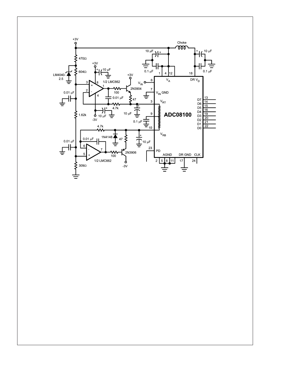
FIGURE 3. Driving the reference to force desired values requires driving with a low impedance source.
ADC08100
www.national.com
15