Applications information – Rainbow Electronics ADC08100 User Manual
Page 14
Applications Information
(Continued)
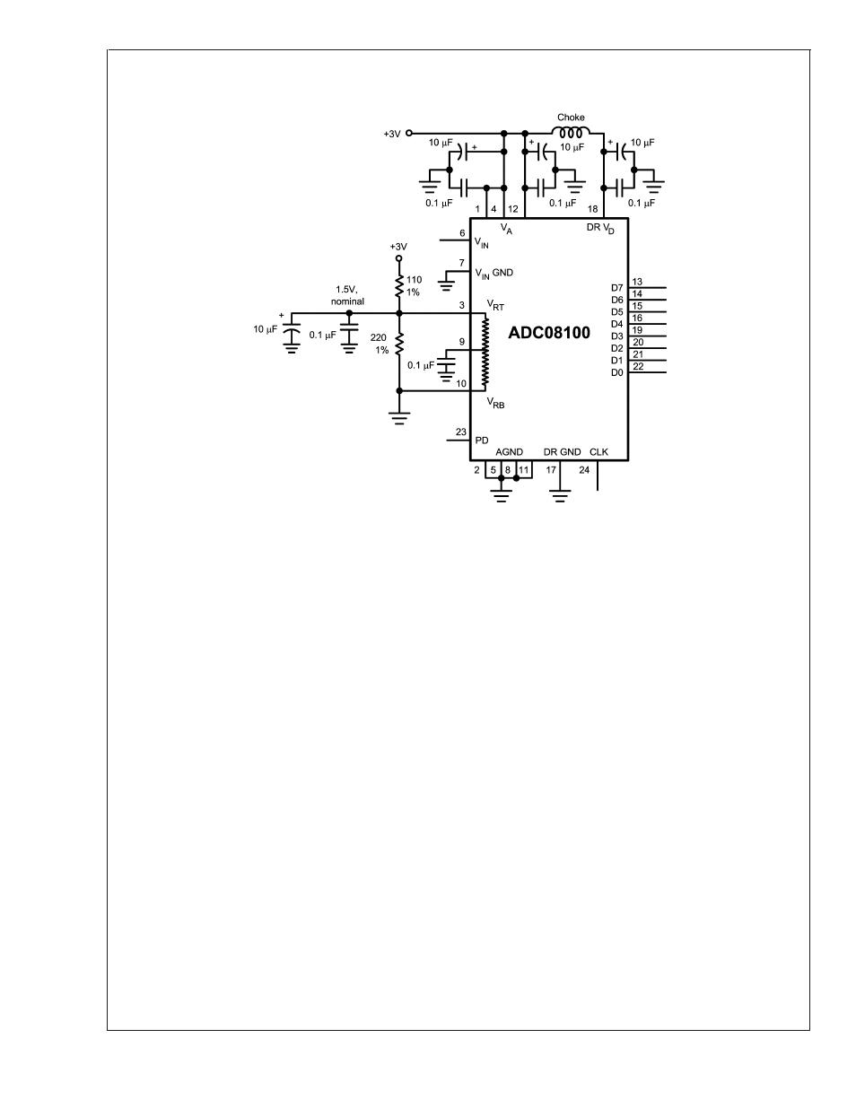
The reference bias circuit of Figure 2 is very simple and the
performance is adequate for many applications. However,
circuit tolerances will lead to a wide reference voltage range.
Superior performance can generally be achieved by driving
the reference pins with a low impedance source.
The circuit of Figure 3 will allow a more accurate setting of
the reference voltages. The lower amplifier must have bipo-
lar supplies as its output voltage must go negative to force
V
RB
to any voltage below the V
BE
of the PNP transistor. Of
course, the divider resistors at the amplifier input could be
changed to suit your reference voltage needs, or the divider
can be replaced with potentiometers for precise settings.
The bottom of the ladder (V
RB
) may simply be returned to
ground if the minimum input signal excursion is 0V. Be sure
that the driving source can source sufficient current into the
V
RT
pin and sink enough current from the V
RB
pin to keep
these pins stable.
The LMC662 amplifier shown was chosen for its low offset
voltage and low cost.
10137132
FIGURE 2. Simple, low component count reference biasing. Because of the ladder and external resistor tolerances,
the reference voltage can vary too much for some applications.
ADC08100
www.national.com
14